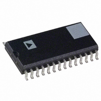
AD73322LAR-REEL Analog Devices Inc, AD73322LAR-REEL Datasheet - Page 2

AD73322LAR-REEL
Manufacturer Part Number
AD73322LAR-REEL
Description
IC ANALOG FRONT END DUAL 28-SOIC
Manufacturer
Analog Devices Inc
Specifications of AD73322LAR-REEL
Rohs Status
RoHS non-compliant
Number Of Bits
16
Number Of Channels
4
Power (watts)
73mW
Voltage - Supply, Analog
2.7 V ~ 5.5 V
Voltage - Supply, Digital
2.7 V ~ 5.5 V
Package / Case
28-SOIC (7.5mm Width)
Single Supply Voltage (min)
2.7V
Single Supply Voltage (max)
3.3V
Package Type
SOIC W
Lead Free Status / RoHS Status
Not Compliant
Parameter
REFERENCE
INPUT AMPLIFIER
ANALOG GAIN TAP
ADC SPECIFICATIONS
DIGITAL GAIN TAP
AD73322L–SPECIFICATIONS
REFCAP
REFOUT
Offset
Maximum Output Swing
Feedback Resistance
Feedback Capacitance
Gain at Maximum Setting
Gain at Minimum Setting
Gain Resolution
Gain Accuracy
Settling Time
Delay
Maximum Input Range at VIN
Nominal Reference Level at VIN
Absolute Gain
Gain Tracking Error
Signal to (Noise + Distortion)
Total Harmonic Distortion
Intermodulation Distortion
Idle Channel Noise Crosstalk
DC Offset
Power Supply Rejection
Group Delay
Input Resistance at PGA
Gain at Maximum Setting
Gain at Minimum Setting
Gain Resolution
Delay
Settling Time
Absolute Voltage, VREFCAP
REFCAP TC
Typical Output Impedance
Absolute Voltage, V
Minimum Load Resistance
Maximum Load Capacitance
(0 dBm0)
PGA = 0 dB
PGA = 0 dB
PGA = 0 dB
ADC-to-DAC
ADC-to-ADC
4, 5
REFOUT
2, 4, 6
2, 3
Min
1.08
–2.0
70
–20
1.08
A, Y Versions
1
Typ
1.2
50
130
1.2
1
100
± 1.0
1.578
50
100
+1
–1
5
± 1.0
1.0
0.5
1.578
–2.85
1.0954
–6.02
–0.7
± 0.1
78
79
77.5
–86
–61
–72
–107
–92
–93
0
–65
25
20
+1
–1
16
25
100
(AVDD = 3 V
16.384 MHz, f
Max
1.32
1.32
+0.5
–75
+20
SAMP
10%; DVDD = 3 V
= 8 kHz; T
Unit
V
ppm/°C 0.1 µF Capacitor Required from
Ω
V
kΩ
pF
mV
V
kΩ
pF
Bits
%
µs
µs
V p-p
dBm
V p-p
dBm
dB
dB
dB
dB
dB
dB
dB
dBm0
dB
dB
dB
mV
dB
µs
kΩ
Bits
µs
µs
A
Test Conditions/Comments
REFCAP to AGND2
Unloaded
Max Output Swing = (1.578/1.2) × VREFCAP
f
Gain Step Size = 0.0625
Output Unloaded
Tap Gain Change of –FS to +FS
DAC Unloaded
Measured Differentially
Max Input = (1.578/1.2) × VREFCAP
Measured Differentially
1.0 kHz, 0 dBm0
1.0 kHz, +3 dBm0 to –50 dBm0
Refer to TPC 1.
300 Hz to 3400 Hz; f
300 Hz to 3400 Hz; f
0 Hz to f
300 Hz to 3400 Hz; f
PGA = 0 dB
PGA = 0 dB
ADC Input Signal Level: 1.0 kHz, 0 dBm0
DAC Input at Idle
ADC1 Input Signal Level: 1.0 kHz, 0 dBm0
ADC2 Input at Idle. Input Amplifiers Bypassed
Input Amplifiers Included in Input Channel
PGA = 0 dB
Input Signal Level at AVDD and DVDD
Pins: 1.0 kHz, 100 mV p-p Sine Wave
Input Amplifiers Bypassed
Tested to 5 MSBs of Settings
Includes DAC Delay
Tap Gain Change from –FS to +FS; Includes
DAC Settling Time
= T
C
= 32 kHz
MIN
to T
10%; DGND = AGND = 0 V, f
SAMP
MAX
, unless otherwise noted.)
/2; f
SAMP
SAMP
SAMP
SAMP
= 8 kHz
= 8 kHz, PUIA = 0
= 8 kHz, PUIA = 1
= 8 kHz
DMCLK
=


