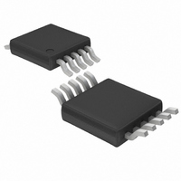
LTC2431CMS#PBF Linear Technology, LTC2431CMS#PBF Datasheet - Page 30

LTC2431CMS#PBF
Manufacturer Part Number
LTC2431CMS#PBF
Description
IC ADC 20BIT DIFFINPUT/REF10MSOP
Manufacturer
Linear Technology
Datasheet
1.LTC2431CMSPBF.pdf
(40 pages)
Specifications of LTC2431CMS#PBF
Number Of Bits
20
Sampling Rate (per Second)
7.5
Data Interface
MICROWIRE™, Serial, SPI™
Number Of Converters
2
Power Dissipation (max)
1mW
Voltage Supply Source
Single Supply
Operating Temperature
0°C ~ 70°C
Mounting Type
Surface Mount
Package / Case
10-TFSOP, 10-MSOP (0.118", 3.00mm Width)
Lead Free Status / RoHS Status
Lead free / RoHS Compliant
Available stocks
Company
Part Number
Manufacturer
Quantity
Price
APPLICATIO S I FOR ATIO
LTC2430/LTC2431
If the F
f
x-axis is scaled by f
ratio f
decrease, but in the same time the LTC2430/LTC2431
noise floor rises and the noise contribution of the driving
amplifiers lose significance.
Normal Mode Rejection and Antialiasing
One of the advantages delta-sigma ADCs offer over con-
ventional ADCs is on-chip digital filtering. Combined with
a large oversampling ratio, the LTC2430/LTC2431 signifi-
cantly simplifies antialiasing filter requirements.
The sinc
mode rejection at all frequencies except DC and integer
multiples of the modulator sampling frequency (f
LTC2430/LTC2431’s autocalibration circuits further sim-
plify the antialiasing requirements by additional normal
mode signal filtering both in the analog and digital domain.
Independent of the operating mode, f
• f
the maximum output data rate. In the internal oscillator
mode, f
15,360Hz with a 60Hz notch setting. In the external
oscillator mode, f
The combined normal mode rejection performance is
shown in Figure 30 for the internal oscillator with 50Hz
notch setting (F
30
EOSC
OUTMAX
, Figure 29 can still be used for noise calculation if the
EOSC
O
S
pin is driven by an external oscillator of frequency
4
Figure 30. Input Normal Mode Rejection,
Internal Oscillator and 50Hz Notch
–100
–110
–120
= 12,800Hz with a 50Hz notch setting and f
digital filter provides greater than 120dB normal
where f
–10
–20
–30
–40
–50
–60
–70
–80
–90
/153600, the Figure 29 plot accuracy begins to
0
0 f
DIFFERENTIAL INPUT SIGNAL FREQUENCY (Hz)
O
S
F
= HIGH) and in Figure 31 for the internal
O
N
2f
S
= HIGH
S
U
is the notch frequency and f
= f
EOSC
3f
S
EOSC
4f
S
/153600. For large values of the
5f
U
S
/10.
6f
S
7f
S
8f
S
W
9f
S
10f
S
S
= 256 • f
11f
2431 F30
S
12f
S
U
OUTMAX
N
S
= 2048
). The
S
is
=
oscillator with F
mode. The regions of low rejection occurring at integer
multiples of f
details of the normal mode rejection curves are shown in
Figure 32 (rejection near DC) and Figure 33 (rejection at
f
These curves have been derived for the external oscillator
mode but they can be used in all operating modes by
appropriately selecting the f
The user can expect to achieve in practice this level of
performance using the internal oscillator as it is demon-
strated by Figures 34 to 36. Typical measured values of the
normal mode rejection of the LTC2430/LTC2431 operat-
ing with an internal oscillator and a 60Hz notch setting are
shown in Figure 34 superimposed over the theoretical
calculated curve. Similarly, typical measured values of the
normal mode rejection of the LTC2430/LTC2431 operat-
ing with an internal oscillator and a 50Hz notch setting are
shown in Figure 35 superimposed over the theoretical
calculated curve.
As a result of these remarkable normal mode specifica-
tions, minimal (if any) antialias filtering is required in front
of the LTC2430/LTC2431. If passive RC components are
placed in front of the LTC2430/LTC2431, the input dy-
namic current should be considered (see Input Current
section). In cases where large effective RC time constants
are used, an external buffer amplifier may be required to
minimize the effects of dynamic input current.
S
–100
–110
–120
= 256f
–10
–20
–30
–40
–50
–60
–70
–80
–90
0
0
DIFFERENTIAL INPUT SIGNAL FREQUENCY (Hz)
Figure 31. Input Normal Mode Rejection, Internal
Oscillator and F
f
S
N
) where f
2f
S
S
3f
have a very narrow bandwidth. Magnified
S
O
4f
= LOW and for the external oscillator
S
5f
O
N
S
= LOW or External Oscillator
6f
represents the notch frequency.
S
7f
S
N
8f
value.
S
9f
2431 F31
S
10f
S
F
F
f
EOSC
O
O
= LOW OR
= EXTERNAL OSCILLATOR,
= 10 • f
S
24301f


