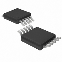
LTC2431CMS#PBF Linear Technology, LTC2431CMS#PBF Datasheet - Page 34

LTC2431CMS#PBF
Manufacturer Part Number
LTC2431CMS#PBF
Description
IC ADC 20BIT DIFFINPUT/REF10MSOP
Manufacturer
Linear Technology
Datasheet
1.LTC2431CMSPBF.pdf
(40 pages)
Specifications of LTC2431CMS#PBF
Number Of Bits
20
Sampling Rate (per Second)
7.5
Data Interface
MICROWIRE™, Serial, SPI™
Number Of Converters
2
Power Dissipation (max)
1mW
Voltage Supply Source
Single Supply
Operating Temperature
0°C ~ 70°C
Mounting Type
Surface Mount
Package / Case
10-TFSOP, 10-MSOP (0.118", 3.00mm Width)
Lead Free Status / RoHS Status
Lead free / RoHS Compliant
Available stocks
Company
Part Number
Manufacturer
Quantity
Price
APPLICATIO S I FOR ATIO
LTC2430/LTC2431
practice in earlier generations of load-cell interfaces, how-
ever the accuracy of the LTC2430/LTC2431 changes the
rationale. Achieving high gain accuracy and linearity at
higher gains may prove difficult, while providing little
benefit in terms of noise reduction.
At a gain of 100, the gain error that could result from
typical open-loop gain of 160dB is –1ppm, however,
worst-case is at the minimum gain of 116dB, giving a gain
error of –158ppm. Worst-case gain error at a gain of 34,
is –54ppm. The use of the LTC1051A reduces the worst-
case gain error to –33ppm. The advantage of gain higher
than 34, then becomes dubious, as the input referred
noise sees little improvement and gain accuracy is poten-
tially compromised.
Note that this 4-amplifier topology has advantages over
the typical integrated 3-amplifier instrumentation ampli-
fier in that it does not have the high noise level common in
the output stage that usually dominates when an instru-
mentation amplifier is used at low gain. If this amplifier is
used at a gain of 10, the gain error is only 10ppm and input
referred noise is reduced to 0.28 V
can also be configured to provide gain of up to 50 with high
gain stability and linearity.
Figure 40 shows an example of a single amplifier used to
produce single-ended gain. This topology is best used in
34
U
BRIDGE
350
U
+
1 F
A
V
Figure 40. Bridge Amplification Using a Single Amplifier
RMS
W
= 9.95 =
. The buffer stages
4.99k
R1
R1 + 175
R1 + R2
U
3
2
–
+
LTC1050
5V
7
4
46.4k
R2
0.1 V
6
applications where the gain setting resistor can be made
to match the temperature coefficient of the strain gauges.
If the bridge is composed of precision resistors, with only
one or two variable elements, the reference arm of the
bridge can be made to act in conjunction with the feedback
resistor to determine the gain. If the feedback resistor is
incorporated into the design of the load cell, using resis-
tors which match the temperature coefficient of the load-
cell elements, good results can be achieved without the
need for resistors with a high degree of absolute accuracy.
The common mode voltage in this case, is again a function
of the bridge output. Differential gain as used with a 350
bridge is:
Common mode gain is half the differential gain. The
maximum differential signal that can be used is 1/4 V
as opposed to 1/2 V
Remote Half Bridge Interface
As opposed to full bridge applications, typical half bridge
applications must contend with nonlinearity in the bridge
output, as signal swing is often much greater. Applications
include RTD’s, thermistors and other resistive elements
that undergo significant changes over their span. For
175
1 F
A
V
+
9 95
.
20k
20k
R
10 F
R
1 175
1
REF
+
REF
REF
IN
IN
R
+
–
in the 2-amplifier topology above.
LTC2430/
LTC2431
+
–
2
GND
V
CC
2431 F40
0.1 F
5V
24301f
REF
,


