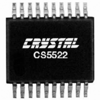
CS5522-ASZ Cirrus Logic Inc, CS5522-ASZ Datasheet - Page 15

CS5522-ASZ
Manufacturer Part Number
CS5522-ASZ
Description
IC ADC 24BIT SIG/DELT 20-SSOP
Manufacturer
Cirrus Logic Inc
Specifications of CS5522-ASZ
Number Of Converters
1
Package / Case
20-SSOP
Number Of Bits
24
Data Interface
Serial
Power Dissipation (max)
14.8mW
Voltage Supply Source
Analog and Digital
Operating Temperature
-40°C ~ 85°C
Mounting Type
Surface Mount
Number Of Adc Inputs
1
Architecture
Delta-Sigma
Conversion Rate
617 SPs
Resolution
24 bit
Input Type
Voltage
Interface Type
Serial (3-Wire)
Voltage Reference
2.5 V
Supply Voltage (max)
5 V
Supply Voltage (min)
25 mV
Maximum Power Dissipation
500 mW
Maximum Operating Temperature
+ 85 C
Mounting Style
SMD/SMT
Input Voltage
25 mV to 5 V
Minimum Operating Temperature
- 40 C
Package
20SSOP
Sampling Rate
0.617 KSPS
Number Of Adcs
1
Number Of Analog Inputs
2
Digital Interface Type
Serial (3-Wire, SPI, Microwire)
Polarity Of Input Voltage
Unipolar|Bipolar
Lead Free Status / RoHS Status
Lead free / RoHS Compliant
Lead Free Status / RoHS Status
Lead free / RoHS Compliant, Lead free / RoHS Compliant
Other names
598-1104-5
Available stocks
Company
Part Number
Manufacturer
Quantity
Price
Part Number:
CS5522-ASZ
Manufacturer:
CIRRUS
Quantity:
20 000
2.1.3 Analog Input Span Considerations
The CS5521/22/23/24/28 is designed to measure
full-scale ranges of 25 mV, 55 mV, 100 mV, 1 V,
2.5 V, and 5 V. Other full scale values can be ac-
commodated by performing a system calibration
within the limits specified. See the Calibration sec-
tion for more details. Another way to change the
full scale range is to increase or to decrease the
voltage reference to a voltage other than 2.5 . See
the Voltage Reference section for more details.
Three factors set the operating limits for the input
span. They include: instrumentation amplifier satu-
ration, modulator 1’s density, and a lower reference
voltage. When the 25 mV, 55 mV, or 100 mV
range is selected, the input signal (including the
common-mode voltage and the amplifier offset
voltage) must not cause the 20X amplifier to satu-
rate in either its input stage or output stage. To pre-
vent saturation, the absolute voltages on AIN+ and
AIN- must stay within the limits specified (refer to
the Analog Input section). Additionally, the differ-
ential output voltage of the amplifier must not ex-
ceed 2.8 V. The equation
defines the differential output limit, where
DS317F4
Note:
Input Range
± 100 mV
± 25 mV
± 55 mV
± 1.0 V
± 2.5 V
± 5.0 V
1. The converter's actual input range, the delta-sigma's nominal full-scale input, and the delta-sigma's
2. The 2.8 V limit at the output of the 20X amplifier is the differential output voltage.
ABS(VIN + VOS) x 20 = 2.8 V
maximum full-scale input all scale directly with the value of the voltage reference. The values in the
table assume a 2.5 V VREF voltage.
Table 1. Relationship between Full Scale Input, Gain Factors, and Internal Analog
VIN = (AIN+) - (AIN-)
(1)
Max. Differential Output
20X Amplifier
2.8 V
2.8 V
2.8 V
-
-
-
(2)
(2)
(2)
Signal Limitations
VREF
2.5V
2.5V
2.5V
2.5V
2.5V
2.5V
is the differential input voltage and VOS is the ab-
solute maximum offset voltage for the instrumenta-
tion amplifier (VOS will not exceed 40 mV). If the
differential output voltage from the amplifier ex-
ceeds 2.8 V, the amplifier may saturate, which will
cause a measurement error.
The input voltage into the modulator must not
cause the modulator to exceed a low of 20 percent
or a high of 80 percent 1's density. The nominal
full-scale input span of the modulator (from 30 per-
cent to 70 percent 1’s density) is determined by the
VREF voltage divided by the Gain Factor. See
Table 1 to determine if the CS5521/22/23/24/28 is
being used properly. For example, in the 55 mV
range, to determine the nominal input voltage to the
modulator, divide VREF (2.5 V) by the Gain Fac-
tor (2.2727).
When a smaller voltage reference is used, the re-
sulting code widths are smaller causing the con-
verter output codes to exhibit more changing codes
for a fixed amount of noise. Table 1 is based upon
a VREF = 2.5 V. For other values of VREF, the
values in Table 1 must be scaled accordingly.
2.1.4 Measuring Voltages Higher than 5 V
Some systems require the measurement of voltages
greater than 5 V. The input current of the instru-
Gain Factor
2.272727...
1.25
2.5
1.0
0.5
5
Differential Input
∆-Σ Nominal
CS5521/22/23/24/28
± 0.5 V
± 1.1 V
± 2.0 V
± 1.0 V
± 2.5 V
± 5.0 V
(1)
Max. Input
± 1.65 V
0V, VA+
± 0.75 V
± 3.0 V
± 1.5 V
± 5.0 V
∆-Σ
(1)
15


