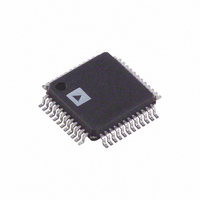
AD7655ASTZ Analog Devices Inc, AD7655ASTZ Datasheet - Page 18

AD7655ASTZ
Manufacturer Part Number
AD7655ASTZ
Description
IC ADC 16BIT 1MSPS QUAD 48-LQFP
Manufacturer
Analog Devices Inc
Series
PulSAR®r
Datasheet
1.AD7655ASTZ.pdf
(28 pages)
Specifications of AD7655ASTZ
Data Interface
Serial, Parallel
Number Of Bits
16
Sampling Rate (per Second)
1M
Number Of Converters
1
Power Dissipation (max)
135mW
Voltage Supply Source
Analog and Digital
Operating Temperature
-40°C ~ 85°C
Mounting Type
Surface Mount
Package / Case
48-LQFP
Resolution (bits)
16bit
Sampling Rate
1MSPS
Input Channel Type
Single Ended
Supply Voltage Range - Analog
4.75V To 5.25V
Package
48LQFP
Resolution
16 Bit
Architecture
SAR
Number Of Adcs
1
Number Of Analog Inputs
4
Digital Interface Type
Parallel|Serial (2-Wire, SPI, QSPI, Microwire)
Input Type
Voltage
Signal To Noise Ratio
86(Typ) dB
Polarity Of Input Voltage
Unipolar
Lead Free Status / RoHS Status
Lead free / RoHS Compliant
For Use With
EVAL-AD7655CBZ - BOARD EVALUATION FOR AD7655
Lead Free Status / RoHS Status
Lead free / RoHS Compliant, Lead free / RoHS Compliant
Available stocks
Company
Part Number
Manufacturer
Quantity
Price
Company:
Part Number:
AD7655ASTZ
Manufacturer:
Analog Devices Inc
Quantity:
10 000
Part Number:
AD7655ASTZ
Manufacturer:
ADI/亚德诺
Quantity:
20 000
Company:
Part Number:
AD7655ASTZRL
Manufacturer:
Analog Devices Inc
Quantity:
10 000
AD7655
CONVERSION CONTROL
Figure 21 shows a detailed timing diagram of the conversion
process. The AD7655 is controlled by the signal CNVST ,
which initiates conversion. Once initiated, it cannot be
restarted or aborted, even by the power-down input, PD,
until the conversion is complete. The CNVST signal operates
independently of the CS and RD signals.
Although CNVST is a digital signal, it should be designed with
special care with fast, clean edges and levels, and with minimum
overshoot and undershoot or ringing.
For applications where the SNR is critical, the CNVST signal
should have very low jitter. One solution is to use a dedicated
oscillator for CNVST generation or, at least, to clock it with a
high frequency low jitter clock, as shown in Figure 17.
In impulse mode, conversions can be automatically initiated. If
CNVST is held low when BUSY is low, the AD7655 controls the
acquisition phase and automatically initiates a new conversion.
By keeping CNVST low, the AD7655 keeps the conversion
process running by itself. Note that the analog input has to be
settled when BUSY goes low. Also, at power-up, CNVST should
be brought low once to initiate the conversion process. In this
mode, the AD7655 can sometimes run slightly faster than the
guaranteed limits of 888 kSPS in impulse mode. This feature
does not exist in normal mode.
DIGITAL INTERFACE
The AD7655 has a versatile digital interface; it can be interfaced
with the host system by using either a serial or parallel interface.
The serial interface is multiplexed on the parallel data bus. The
AD7655 digital interface accommodates either 3 V or 5 V logic
when the OVDD supply pin of the AD7655 is connected to the
host system interface digital supply.
MODE
CNVST
BUSY
EOC
A0
ACQUIRE
t
t
t
10
5
3
CONVERT A
t
1
Figure 21. Basic Conversion Timing
t
11
t
12
t
t
4
7
CONVERT B
t
2
t
13
ACQUIRE
t
6
t
t
8
14
CONVERT
t
15
Rev. B | Page 18 of 28
The two signals, CS and RD , control the interface. When at
least one of these signals is high, the interface outputs are in
high impedance. Usually CS allows the selection of each
AD7655 in multicircuit applications and is held low in a single
AD7655 design. RD is generally used to enable the conversion
result on the data bus. In parallel mode, signal A/ B allows the
choice of reading either the output of Channel A or Channel B,
whereas in serial mode, signal A/ B controls which channel is
output first.
Figure 22 details the timing when using the RESET input. Note
the current conversion, if any, is aborted and the data bus is
high impedance while RESET is high.
PARALLEL INTERFACE
The AD7655 is configured to use the parallel interface when
SER/ PAR is held low.
Master Parallel Interface
Data can be read continuously by tying CS and RD low, thus
requiring minimal microprocessor connections. However, in
this mode the data bus is always driven and cannot be used in
shared bus applications (unless the device is held in RESET).
Figure 23 details the timing for this mode.
CNVST
CNVST
RESET
CS = RD = 0
BUSY
DATA
BUSY
DATA
EOC
BUS
BUS
Figure 23. Master Parallel Data Timing for Reading (Continuous Read)
t
t
10
3
PREVIOUS CHANNEL A
OR B
t
1
Figure 22. Reset Timing
t
9
PREVIOUS CHANNEL B
t
16
OR NEW A
t
t
8
4
t
17
NEW A
OR B


