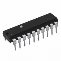
ADC0838CCN/NOPB National Semiconductor, ADC0838CCN/NOPB Datasheet - Page 17

ADC0838CCN/NOPB
Manufacturer Part Number
ADC0838CCN/NOPB
Description
IC ADC 8BIT SERIAL I/O 20-DIP
Manufacturer
National Semiconductor
Datasheet
1.ADC0831CCWMNOPB.pdf
(33 pages)
Specifications of ADC0838CCN/NOPB
Number Of Bits
8
Sampling Rate (per Second)
31k
Data Interface
NSC MICROWIRE™, Serial
Number Of Converters
1
Power Dissipation (max)
15mW
Voltage Supply Source
Single Supply
Operating Temperature
0°C ~ 70°C
Mounting Type
Through Hole
Package / Case
20-DIP (0.300", 7.62mm)
Lead Free Status / RoHS Status
Lead free / RoHS Compliant
Other names
*ADC0838CCN
*ADC0838CCN/NOPB
ADC0838
ADC0838CCN
*ADC0838CCN/NOPB
ADC0838
ADC0838CCN
Functional Description
possible because the DI input is only “looked-at” during the
MUX addressing interval while the DO line is still in a high
impedance state.
3.0 Reference Considerations
The voltage applied to the reference input to these convert-
ers defines the voltage span of the analog input (the differ-
ence between V
possible output codes apply. The devices can be used in
either ratiometric applications or in systems requiring abso-
lute accuracy. The reference pin must be connected to a
voltage source capable of driving the reference input resis-
tance of typically 3.5 kΩ. This pin is the top of a resistor
divider string used for the successive approximation conver-
sion.
In a ratiometric system, the analog input voltage is propor-
tional to the voltage used for the A/D reference. This voltage
is typically the system power supply, so the V
4.0 The Analog Inputs
The most important feature of these converters is that they
can be located right at the analog signal source and through
just a few wires can communicate with a controlling proces-
sor with a highly noise immune serial bit stream. This in itself
greatly minimizes circuitry to maintain analog signal accu-
racy which otherwise is most susceptible to noise pickup.
However, a few words are in order with regard to the analog
inputs should the input be noisy to begin with or possibly
riding on a large common-mode voltage.
The differential input of these converters actually reduces
the effects of common-mode input noise, a signal common
to both selected “+” and “−” inputs for a conversion (60 Hz is
most typical). The time interval between sampling the “+”
input and then the “−” input is
change in the common-mode voltage during this short time
interval can cause conversion errors. For a sinusoidal
common-mode signal this error is:
IN(MAX)
a) Ratiometric
and V
IN(MIN)
1
⁄
2
of a clock period. The
) over which the 256
(Continued)
00558357
REF
FIGURE 2. Reference Examples
pin can be
17
tied to V
relaxes the stability requirements of the system reference as
the analog input and A/D reference move together maintain-
ing the same output code for a given input condition.
For absolute accuracy, where the analog input varies be-
tween very specific voltage limits, the reference pin can be
biased with a time and temperature stable voltage source.
The LM385 and LM336 reference diodes are good low cur-
rent devices to use with these converters.
The maximum value of the reference is limited to the V
supply voltage. The minimum value, however, can be quite
small (see Typical Performance Characteristics) to allow
direct conversions of transducer outputs providing less than
a 5V output span. Particular care must be taken with regard
to noise pickup, circuit layout and system error voltage
sources when operating with a reduced span due to the
increased sensitivity of the converter (1 LSB equals
V
where f
For a 60 Hz common-mode signal to generate a
(≈5 mV) with the converter running at 250 kHz, its peak value
would have to be 6.63V which would be larger than allowed
as it exceeds the maximum analog input limits.
Due to the sampling nature of the analog inputs short spikes
of current enter the “+” input and exit the “−” input at the
clock edges during the actual conversion. These currents
decay rapidly and do not cause errors as the internal com-
parator is strobed at the end of a clock period. Bypass
capacitors at the inputs will average these currents and
cause an effective DC current to flow through the output
REF
V
and f
PEAK
/256).
CM
CLK
CC
is its peak voltage value
, is the A/D clock frequency.
is the frequency of the common-mode signal,
(done internally on the ADC0832). This technique
b) Absolute with a reduced Span
1
www.national.com
⁄
4
00558358
LSB error
CC


