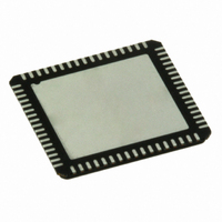
ADC16DV160CILQ/NOPB National Semiconductor, ADC16DV160CILQ/NOPB Datasheet - Page 23

ADC16DV160CILQ/NOPB
Manufacturer Part Number
ADC16DV160CILQ/NOPB
Description
ADC 16BIT DUAL 160MSPS 68LLP
Manufacturer
National Semiconductor
Series
PowerWise®r
Datasheet
1.ADC16DV160CILQNOPB.pdf
(30 pages)
Specifications of ADC16DV160CILQ/NOPB
Number Of Bits
16
Sampling Rate (per Second)
160M
Data Interface
Serial, SPI™
Number Of Converters
2
Power Dissipation (max)
1.47W
Voltage Supply Source
Single Supply
Operating Temperature
-40°C ~ 85°C
Mounting Type
Surface Mount
Package / Case
68-VFQFN, Exposed Pad
Leaded Process Compatible
Yes
Rohs Compliant
Yes
Peak Reflow Compatible (260 C)
Yes
Lead Free Status / RoHS Status
Lead free / RoHS Compliant
Other names
ADC16DV160CILQ
Signal Descriptions
SCLK: Used to register the input date (SDI) on the rising
CSB:
SDIO: Serial Data. Must observe setup/hold requirements
For flexibility, the user can determine a fixed pattern with a
depth of 8 patterns as shown in
these 8 sequences (SEQ0 – SEQ7) with an arbitrary pattern
(PATTERN (000) – PATTERN (111)). See Register Map ad-
dress 08h through 0Bh below for the details. The default
edge; and to source the output data (SDO) on the
falling edge. User may disable clock and hold it in the
low-state, as long as clock pulse width min. spec is
not violated when clock is enabled or disabled.
Chip Select Bar. Each assertion starts a new register
access – i.e., the SDATA field protocol is required.
CSB should be de-asserted after the 16th clock. If the
CSB is de-asserted before the 16th clock, no address
or data write will occur. The rising edge captures the
address just shifted-in and, in the case of a write op-
eration, writes the addressed register.
with respect to the SCLK. Each cycle is 16-bit long.
Figure
FIGURE 15. Serial Interface Protocol (Read Operation)
17. The user can fill
FIGURE 16. Fixed Pattern Map
23
•
•
•
•
9.0 FIXED PATTERN MODE
The ADC16DV160 provides user defined fixed patterns at
digital output pins to check timing and connectivity with the
receiving device on the board. The fixed pattern map is shown
in
(000) to PATTERN (101)) and 2 user-defined patterns (PAT-
TERN (110) and PATTERN (111)). PATTERN (110) and
PATTERN (111) can be written via SPI and all ‘0’s are the
default values for both. See Register Map address 0CH
through 0FH for the details.
register value for all SEQ0 through SEQ7 sequences is 010,
which generates alternating 0xFF and 0x00 at the ADC output
as shown in
bits on the falling edge of the OUTCLK and even bits on the
rising edge, the resulting 16-bit output codes are 0xAAAA.
Figure
R/W: A value of ‘1’ indicates a read operation, while a
value of ‘0’ indicates a write operation
Reserved: Reserved for future use. Must be set to 0.
ADDR: Up to 64 registers can be addressed.
DATA: In a write operation the value in this field will be
written to the register addressed in this cycle when CSB
is de-asserted. In a read operation this field is ignored.
16; there are 6 hard-wired fixed patterns (PATTERN
Figure
18. Note that since the ADC outputs odd
30101453
30101452
www.national.com


