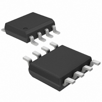
MAX1243BESA+ Maxim Integrated Products, MAX1243BESA+ Datasheet - Page 10

MAX1243BESA+
Manufacturer Part Number
MAX1243BESA+
Description
IC ADC 10BIT SERIAL 8-SOIC
Manufacturer
Maxim Integrated Products
Datasheet
1.MAX1243BCSA.pdf
(12 pages)
Specifications of MAX1243BESA+
Number Of Bits
10
Sampling Rate (per Second)
73k
Data Interface
MICROWIRE™, QSPI™, Serial, SPI™
Number Of Converters
1
Power Dissipation (max)
471mW
Voltage Supply Source
Single Supply
Operating Temperature
-40°C ~ 85°C
Mounting Type
Surface Mount
Package / Case
8-SOIC (0.154", 3.90mm Width)
Number Of Adc Inputs
1
Architecture
SAR
Conversion Rate
73 KSPs
Resolution
10 bit
Input Type
Voltage
Interface Type
Serial
Voltage Reference
External
Supply Voltage (max)
5 V
Maximum Power Dissipation
471 mW
Maximum Operating Temperature
+ 85 C
Mounting Style
SMD/SMT
Minimum Operating Temperature
- 40 C
Lead Free Status / RoHS Status
Lead free / RoHS Compliant
+2.7V to +5.25V, Low-Power, 10-Bit
Serial ADCs in SO-8
The actual conversion does not require the external
clock. This allows the conversion result to be read back
at the µP’s convenience at any clock rate up to
2.1MHz. The clock duty cycle is unrestricted if each
clock phase is at least 200ns. Do not run the clock
while a conversion is in progress.
Conversion-start and data-read operations are con-
trolled by the CS and SCLK digital inputs. The timing
diagrams of Figures 8 and 9 outline serial-interface
operation.
A CS falling edge initiates a conversion sequence: the
T/H stage holds the input voltage, the ADC begins to
convert, and DOUT changes from high impedance to
logic low. SCLK must be kept low during the conver-
sion. An internal register stores the data when the con-
version is in progress.
EOC is signaled by DOUT going high. DOUT’s rising
edge can be used as a framing signal. SCLK shifts the
data out of this register any time after the conversion is
complete. DOUT transitions on SCLK’s falling edge.
The next falling clock edge produces the MSB of the
conversion at DOUT, followed by the remaining bits.
Since there are 10 data bits, two sub-bits, and one
leading high bit, at least 13 falling clock edges are
needed to shift out these bits. Extra clock pulses occur-
ring after the conversion result has been clocked out,
and prior to a rising edge of CS, produce trailing zeros
at DOUT and have no effect on converter operation.
For minimum cycle time, use DOUT’s rising edge as
the EOC signal and then clock out the data with 10.5
clock cycles at full speed (Figure 8b). Pull CS high after
reading the conversion’s LSB. After the specified mini-
mum time, t
conversion.
The data output from the MAX1242/MAX1243 is binary.
Figure 10 depicts the nominal transfer function. Code
transitions occur halfway between successive-integer
LSB values. If V
2.5V / 1024.
The MAX1242/MAX1243 serial interface is fully compat-
ible with SPI, QSPI, and Microwire standard serial inter-
faces (Figure 11).
10
__________Applications Information
______________________________________________________________________________________
Output Coding and Transfer Function
Connection to Standard Interfaces
CS
, pull CS low again to initiate the next
REF
= 2.5V, then 1LSB = 2.44mV or
Timing and Control
External Clock
Figure 10. Unipolar Transfer Function, Full Scale (FS) =
V
Figure 11. Common Serial-Interface Connections to the
MAX1242/MAX1243
REF
- 1LSB, Zero Scale (ZS) = GND
11 111
11 110
11 101
00 011
00 010
00 001
00 000
a) SPI
b) QSPI
c) MICROWIRE
OUTPUT CODE
0
MISO
MISO
1
SCK
SCK
I/O
CS
I/O
SS
SS
SK
SI
INPUT VOLTAGE (LSB)
2
3
+3V
+3V
FULL-SCALE
TRANSITION
CS
SCLK
DOUT
CS
SCLK
DOUT
CS
SCLK
DOUT
FS - 3/2LSB
MAX1242
MAX1243
MAX1242
MAX1243
MAX1242
MAX1243
FS = V
1LSB =
FS
REF
1024
V
REF
- 1LSB


