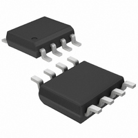
MAX1243BESA+ Maxim Integrated Products, MAX1243BESA+ Datasheet - Page 11

MAX1243BESA+
Manufacturer Part Number
MAX1243BESA+
Description
IC ADC 10BIT SERIAL 8-SOIC
Manufacturer
Maxim Integrated Products
Datasheet
1.MAX1243BCSA.pdf
(12 pages)
Specifications of MAX1243BESA+
Number Of Bits
10
Sampling Rate (per Second)
73k
Data Interface
MICROWIRE™, QSPI™, Serial, SPI™
Number Of Converters
1
Power Dissipation (max)
471mW
Voltage Supply Source
Single Supply
Operating Temperature
-40°C ~ 85°C
Mounting Type
Surface Mount
Package / Case
8-SOIC (0.154", 3.90mm Width)
Number Of Adc Inputs
1
Architecture
SAR
Conversion Rate
73 KSPs
Resolution
10 bit
Input Type
Voltage
Interface Type
Serial
Voltage Reference
External
Supply Voltage (max)
5 V
Maximum Power Dissipation
471 mW
Maximum Operating Temperature
+ 85 C
Mounting Style
SMD/SMT
Minimum Operating Temperature
- 40 C
Lead Free Status / RoHS Status
Lead free / RoHS Compliant
If a serial interface is available, set the CPU’s serial
interface in master mode so the CPU generates the ser-
ial clock. Choose a clock frequency up to 2.1MHz.
1) Use a general-purpose I/O line on the CPU to pull CS
2) Wait the maximum conversion time specified before
3) Activate SCLK for a minimum of 11 clock cycles. The
4) Pull CS high at or after the 11th falling clock edge. If
5) With CS = high, wait the minimum specified time, t
Data can be output in two bytes or continuously, as
shown in Figures 8a and 8b. The bytes contain the
result of the conversion padded with one leading 1, two
sub-bits, and trailing 0s if SCLK is still active with CS
kept low.
Figure 12. SPI/Microwire Serial-Interface Timing (CPOL = CPHA = 0)
Figure 13. QSPI Serial-Interface Timing (CPOL = CPHA = 0)
low. Keep SCLK low.
activating SCLK. Alternatively, look for a DOUT rising
edge to determine the end of conversion.
first falling clock edge produces the MSB of the
DOUT conversion. DOUT output data transitions on
SCLK’s falling edge and is available in MSB-first for-
mat. Observe the SCLK-to-DOUT valid timing char-
acteristic. Data can be clocked into the µP on
SCLK’s rising edge.
CS remains low, the two sub-bits and trailing zeros
are clocked out after the LSB.
before initiating a new conversion by pulling CS low.
If a conversion is aborted by pulling CS high before
the conversion’s end, wait the minimum acquisition
time, t
DOUT
SCLK
CS
ACQ
t
CONV
, before starting a new conversion.
DOUT
SCLK
EOC
CS
______________________________________________________________________________________
t
CONV
MSB
D9
EOC
D8
+2.7V to +5.25V, Low-Power, 10-Bit
1ST BYTE READ
D7
MSB
D9
D6
D5
D8
D7
D4
CS
D6
D3
,
D5
When using SPI or QSPI, set CPOL = 0 and CPHA = 0.
Conversion begins with a CS falling edge. DOUT goes
low, indicating a conversion is in progress. Wait until
DOUT goes high or until the maximum specified 7.5µs
conversion time elapses. Two consecutive 1-byte reads
are required to get the full 10+2 bits from the ADC.
DOUT output data transitions on SCLK’s falling edge
and is clocked into the µP on SCLK’s rising edge.
The first byte contains a leading 1, and seven bits of
conversion result. The second byte contains the remain-
ing three bits, two sub-bits, and three trailing zeros. See
Figure 11 for connections and Figure 12 for timing.
Set CPOL = CPHA = 0. Unlike SPI, which requires two
1-byte reads to acquire the 10 bits of data from the ADC,
QSPI allows the minimum number of clock cycles neces-
sary to clock in the data. The MAX1242/MAX1243 require
11 clock cycles from the µP to clock out the 10 bits of
data. Additional clock cycles clock out the two sub-bits
followed by trailing zeros (Figure 13). The maximum clock
frequency to ensure compatibility with QSPI is 2.097MHz.
For best performance, use printed circuit boards. Wire-
wrap boards are not recommended. Board layout
should ensure that digital and analog signal lines are
separated from each other. Do not run analog and digi-
tal (especially clock) lines parallel to one another, or
digital lines underneath the ADC package.
D4
D2
D3
Serial ADCs in SO-8
D2
D1
D1
LSB
D0
LSB
D0
2ND BYTE READ
S1
S1
Layout and Grounding
S0
S0
SPI and Microwire
HIGH-Z
QSPI
HIGH-Z
11


