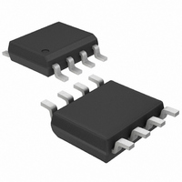
MAX1243BESA+ Maxim Integrated Products, MAX1243BESA+ Datasheet - Page 4

MAX1243BESA+
Manufacturer Part Number
MAX1243BESA+
Description
IC ADC 10BIT SERIAL 8-SOIC
Manufacturer
Maxim Integrated Products
Datasheet
1.MAX1243BCSA.pdf
(12 pages)
Specifications of MAX1243BESA+
Number Of Bits
10
Sampling Rate (per Second)
73k
Data Interface
MICROWIRE™, QSPI™, Serial, SPI™
Number Of Converters
1
Power Dissipation (max)
471mW
Voltage Supply Source
Single Supply
Operating Temperature
-40°C ~ 85°C
Mounting Type
Surface Mount
Package / Case
8-SOIC (0.154", 3.90mm Width)
Number Of Adc Inputs
1
Architecture
SAR
Conversion Rate
73 KSPs
Resolution
10 bit
Input Type
Voltage
Interface Type
Serial
Voltage Reference
External
Supply Voltage (max)
5 V
Maximum Power Dissipation
471 mW
Maximum Operating Temperature
+ 85 C
Mounting Style
SMD/SMT
Minimum Operating Temperature
- 40 C
Lead Free Status / RoHS Status
Lead free / RoHS Compliant
TIMING CHARACTERISTICS
(V
+2.7V to +5.25V, Low-Power, 10-Bit
Serial ADCs in SO-8
Note 1: Tested at V
Note 2: Relative accuracy is the deviation of the analog value at any code from its theoretical value after the full-scale range and
Note 3: Offset nulled.
Note 4: Sample tested to 0.1% AQL.
Note 5: External load should not change during conversion for specified accuracy.
Note 6: Guaranteed by design. Not subject to production testing.
Note 7: Measured as [V
Note 8: To guarantee acquisition time, t
Figure 1. Load Circuits for DOUT Enable Time
Figure 2. Load Circuits for DOUT Disable Time
4
Acquisition Time
SCLK Fall to Output Data Valid
CS Fall to Output Enable
CS Rise to Output Disable
SCLK Clock Frequency
SCLK Pulse Width High
SCLK Pulse Width Low
SCLK Low to CS Fall Setup Time
DOUT Rise to SCLK Rise (Note 6)
CS Pulse Width
DD
_______________________________________________________________________________________
= +2.7V to +5.25V, circuit of Figure 9, T
a) High-Z to V
offset have been calibrated.
time needed for the signal to be acquired.
a) V
PARAMETER
DOUT
DOUT
OH
to High-Z
OH
DD
and V
6k
6k
= +2.7V.
FS
OL
to V
(V
DGND
DGND
OH
DD (min)
SYMBOL
) - V
f
t
SCLK
t
t
ACQ
t
t
t
t
CS0
t
t
STR
DO
CH
DV
TR
CL
CS
ACQ
FS
(V
A
is the maximum time the device takes to acquire the signal, and is also the minimum
DD (max)
= T
CS = V
Figure 1,
C
Figure 1, C
Figure 2, C
C
LOAD
C
LOAD
MIN
LOAD
)].
= 50pF
to T
= 50pF
DD
= 50pF
MAX
(Note 8)
LOAD
LOAD
, unless otherwise noted.)
CONDITIONS
= 50pF
= 50pF
MAX124_ _C/E
MAX124_ _M
b) High-Z to V
b) V
OL
DOUT
DOUT
to High-Z
OL
and V
OH
to V
MIN
200
200
240
1.5
20
20
50
+2.7V
0
0
+2.7V
OL
6k
6k
DGND
DGND
C
C
LOAD
LOAD
TYP
= 50pF
= 50pF
MAX
200
240
240
240
2.1
UNITS
MHz
µs
ns
ns
ns
ns
ns
ns
ns
ns


