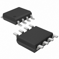
MAX1243BESA+ Maxim Integrated Products, MAX1243BESA+ Datasheet - Page 3

MAX1243BESA+
Manufacturer Part Number
MAX1243BESA+
Description
IC ADC 10BIT SERIAL 8-SOIC
Manufacturer
Maxim Integrated Products
Datasheet
1.MAX1243BCSA.pdf
(12 pages)
Specifications of MAX1243BESA+
Number Of Bits
10
Sampling Rate (per Second)
73k
Data Interface
MICROWIRE™, QSPI™, Serial, SPI™
Number Of Converters
1
Power Dissipation (max)
471mW
Voltage Supply Source
Single Supply
Operating Temperature
-40°C ~ 85°C
Mounting Type
Surface Mount
Package / Case
8-SOIC (0.154", 3.90mm Width)
Number Of Adc Inputs
1
Architecture
SAR
Conversion Rate
73 KSPs
Resolution
10 bit
Input Type
Voltage
Interface Type
Serial
Voltage Reference
External
Supply Voltage (max)
5 V
Maximum Power Dissipation
471 mW
Maximum Operating Temperature
+ 85 C
Mounting Style
SMD/SMT
Minimum Operating Temperature
- 40 C
Lead Free Status / RoHS Status
Lead free / RoHS Compliant
reference; V
ELECTRICAL CHARACTERISTICS (continued)
(V
EXTERNAL REFERENCE (VREF = 2.5V)
DIGITAL INPUTS: SCLK, C C S S , S S H H D D N N
INTERNAL REFERENCE (MAX1242 only)
REF Output Voltage
REF Short-Circuit Current
REF Temperature Coefficient
Load Regulation (Note 5)
Capacitive Bypass at REF
Input Voltage Range
Input Current
Input Resistance
REF Input Current in Shutdown
Capacitive Bypass at REF
SCLK,
SCLK, CS Input Low Voltage
SCLK, CS Input Hysteresis
SCLK, CS Input Leakage
SCLK, CS Input Capacitance
SHDN Input High Voltage
SHDN Input Low Voltage
SHDN Input Current
SHDN Input Mid Voltage
SHDN Voltage, Floating
SHDN Max Allowed Leakage,
Mid Input
DIGITAL OUTPUT: DOUT
Output Voltage Low
Output Voltage High
Three-State Leakage Current
Three-State Output Capacitance
POWER REQUIREMENTS
Supply Voltage
Supply Current
Power-Supply Rejection (Note 7)
DD
= +2.7V to +5.25V; 73ksps; f
CS Input High Voltage
PARAMETER
REF
= 2.5V applied to REF pin; T
_______________________________________________________________________________________
SYMBOL
+2.7V to +5.25V, Low-Power, 10-Bit
SCLK
V
C
V
V
V
V
PSR
V
V
V
V
HYST
C
I
V
I
OUT
DD
FLT
I
IN
SM
OH
DD
SH
OL
SL
IH
L
IL
IN
= 2.1MHz (50% duty cycle); MAX1242—4.7µF capacitor at REF pin, MAX1243—external
A
= T
Operating mode (MAX1242)
T
MAX1242
0mA to 0.2mA output load
SHDN = 0V
V
V
(Note 6)
SHDN = 0V or V
SHDN = float
SHDN = float
I
I
CS = V
CS = V
Operating mode (MAX1242)
Operating mode (MAX1243)
Power-down
V
V
I
SINK
SINK
SOURCE
A
DD
DD
IN
DD
MIN
= +25°C (Note 4)
= 0V or V
> 3.6V
= V
≤ 3.6V
= 5MA
= 16mA
to T
DD
DD
DD (min)
= 0.5mA
MAX
(Note 6)
DD
; unless otherwise noted.)
CONDITIONS
to V
DD
DD (max)
, full-scale input
Serial ADCs in SO-8
V
V
V
V
V
V
DD
DD
DD
DD
DD
DD
= 3.6V
= 5.25V
= 5.25V
= 5.25V
= 3.6V
= 3.6V
V
V
2.470
DD
DD
1.00
MIN
4.7
0.1
2.0
3.0
1.1
2.7
18
- 0.4
- 0.5
V
±0.01
±0.01
±0.01
2.500
DD
±0.3
TYP
0.35
±30
100
0.2
1.4
1.8
0.9
1.6
1.9
3.5
25
/ 2
V
DD
V
2.530
50mV
±100
MAX
±4.0
5.25
±10
150
DD
0.8
0.4
0.4
0.8
2.0
3.0
1.5
2.5
±1
30
10
15
15
10
15
- 1.1
+
ppm/°C
UNITS
mA
mV
mA
µA
kΩ
µA
µA
µA
nA
µA
µA
µF
µF
pF
pF
mV
V
V
V
V
V
V
V
V
V
V
V
V
3


