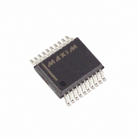
MAX148BCAP+ Maxim Integrated Products, MAX148BCAP+ Datasheet - Page 11

MAX148BCAP+
Manufacturer Part Number
MAX148BCAP+
Description
IC ADC SRL 8CH 10BIT LP 20-SSOP
Manufacturer
Maxim Integrated Products
Datasheet
1.MAX148BCAP.pdf
(23 pages)
Specifications of MAX148BCAP+
Number Of Bits
10
Sampling Rate (per Second)
133k
Data Interface
MICROWIRE™, QSPI™, Serial, SPI™
Number Of Converters
1
Power Dissipation (max)
640mW
Voltage Supply Source
Single Supply
Operating Temperature
0°C ~ 70°C
Mounting Type
Surface Mount
Package / Case
20-SSOP
Number Of Adc Inputs
8
Architecture
SAR
Conversion Rate
133 KSPs
Resolution
10 bit
Input Type
Voltage
Interface Type
4-Wire (SPI, QSPI, MICROWIRE, TMS320)
Voltage Reference
Internal 2.5 V or External
Supply Voltage (max)
5 V
Maximum Power Dissipation
640 mW
Maximum Operating Temperature
+ 70 C
Mounting Style
SMD/SMT
Minimum Operating Temperature
0 C
Lead Free Status / RoHS Status
Lead free / RoHS Compliant
Table 3. Channel Selection in Differential Mode (SGL/DIF = 0)
Make sure the CPU’s serial interface runs in master
mode so the CPU generates the serial clock. Choose a
clock frequency from 100kHz to 2MHz.
Figure 6. 24-Clock External Clock Mode Conversion Timing (MICROWIRE and SPI-Compatible, QSPI-Compatible with f SCLK P 2MHz)
1) Set up the control byte for external clock mode and
2) Use a general-purpose I/O line on the CPU to pull CS
3) Transmit TB1 and, simultaneously, receive a byte
4) Transmit a byte of all zeros ($00 hex) and, simultane-
5) Transmit a byte of all zeros ($00 hex) and, simultane-
6) Pull CS high.
A/D STATE
SEL2
SSTRB
call it TB1. TB1 should be of the format: 1XXXXX11
binary, where the Xs denote the particular channel
and conversion mode selected.
low.
and call it RB1. Ignore RB1.
ously, receive byte RB2.
ously, receive byte RB3.
DOUT
SCLK
0
0
0
0
1
1
1
1
DIN
CS
SEL1
START
0
0
1
1
0
0
1
1
1
______________________________________________________________________________________
SEL2 SEL1 SEL0
+2.7V to +5.25V, Low-Power, 8-Channel,
SEL0
0
1
0
1
0
1
0
1
IDLE
4
RB1
Simple Software Interface
UNI/
BIP
SGL/
DIF
(f
ACQUISITION
SCLK
CH0
1.5Fs
+
PD1
t
-
ACQ
= 2MHz)
PD0
8
CH1
+
-
MSB
B9
B8
CH2
+
-
B7
12
RB2
Figure 6 shows the timing for this sequence. Bytes RB2
and RB3 contain the result of the conversion, padded
with one leading zero, two sub-LSB bits, and three
trailing zeros. The total conversion time is a function of
the serial-clock frequency and the amount of idle time
between 8-bit transfers. To avoid excessive T/H droop,
make sure the total conversion time does not exceed
120Fs.
In unipolar input mode, the output is straight binary
(Figure 17). For bipolar input mode, the output is twos
complement (Figure 18). Data is clocked out at the fall-
ing edge of SCLK in MSB-first format.
The MAX148/MAX149 may use either an external serial
clock or the internal clock to perform the successive-
approximation conversion. In both clock modes, the exter-
nal clock shifts data in and out of the MAX148/MAX149.
B6
CONVERSION
B5
CH3
+
-
B4
Serial 10-Bit ADCs
B3
16
CH4
+
B2
-
B1
LSB
CH5
B0
+
-
S1
20
RB3
S0
IDLE
FILLED WITH
ZEROS
CH6
+
Clock Modes
-
Digital Output
24
CH7
+
-
11


