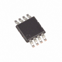
MAX145ACUA+ Maxim Integrated Products, MAX145ACUA+ Datasheet - Page 10

MAX145ACUA+
Manufacturer Part Number
MAX145ACUA+
Description
IC ADC 12BIT 108KSPS 8-UMAX
Manufacturer
Maxim Integrated Products
Datasheet
1.MAX144BEUA.pdf
(16 pages)
Specifications of MAX145ACUA+
Number Of Bits
12
Sampling Rate (per Second)
108k
Data Interface
MICROWIRE™, QSPI™, Serial, SPI™
Number Of Converters
1
Power Dissipation (max)
330mW
Voltage Supply Source
Single Supply
Operating Temperature
0°C ~ 70°C
Mounting Type
Surface Mount
Package / Case
8-TSSOP, 8-MSOP (0.118", 3.00mm Width)
Lead Free Status / RoHS Status
Lead free / RoHS Compliant
An external reference is required for both the MAX144
and the MAX145. At REF, the DC input resistance is a
minimum of 18kΩ. During a conversion, a reference
must be able to deliver 250µA of DC load current and
have an output impedance of 10Ω or less. Use a 0.1µF
bypass capacitor for best performance. The reference
input structure allows a voltage range of 0 to V
50mV, although noise levels will decrease effective res-
olution at lower reference voltages.
Whenever the MAX144/MAX145 are not selected
(CS/SHDN = V
mode. In shutdown all internal circuitry turns off, reduc-
ing supply current to typically less than 0.2µA. With an
external reference stable to within 1LSB, the wake-up
time is 2.5µs. If the external reference is not stable with-
in 1LSB, the wake-up time must be increased to allow
the reference to stabilize.
For a waveform perfectly reconstructed from digital
samples, the theoretical maximum SNR is the ratio of
full-scale analog input (RMS value) to the RMS quanti-
zation error (residual error). The ideal, theoretical mini-
mum analog-to-digital noise is caused by quantization
error only and results directly from the ADC’s resolution
(N bits):
In reality, there are other noise sources besides quanti-
zation noise: thermal noise, reference noise, clock jitter,
etc. Therefore, SNR is computed by taking the ratio of
the RMS signal to the RMS noise which includes all
spectral components minus the fundamental, the first
five harmonics, and the DC offset.
SINAD is the ratio of the fundamental input frequency’s
RMS amplitude to RMS equivalent of all other ADC out-
put signals:
+2.7V, Low-Power, 2-Channel, 108ksps,
Serial 12-Bit ADCs in 8-Pin µMAX
Table 1. Serial Output Data Stream for Internal and External Clock Mode
__________Applications Information
10
DOUT (Internal Clock)
DOUT (External Clock)
SINAD(dB) = 20 x log
______________________________________________________________________________________
Signal-to-Noise Plus Distortion (SINAD)
SCLK CYCLE
SNR
DD
(MAX)
Automatic Power-Down Mode
), the parts enter their shutdown
Signal-to-Noise Ratio (SNR)
= (6.02 x N + 1.76)dB
(Noise + Distortion)
EOC
1
1
External Reference
SIGNAL
2
1
1
RMS
3
1
1
CHID D11 D10
CHID D11 D10
RMS
4
DD
5
+
6
ENOB indicates the global accuracy of an ADC at a
specific input frequency and sampling rate. An ideal
ADC’s error consists only of quantization noise. With an
input range equal to the full-scale range of the ADC, the
effective number of bits can be calculated as follows:
THD is the ratio of the RMS sum of the first five harmon-
ics of the input signal to the fundamental itself. This is
expressed as:
where V
V
harmonics.
SFDR is the ratio of RMS amplitude of the fundamental
(maximum signal component) to the RMS value of the
next largest spurious component, excluding DC offset.
The MAX144/MAX145 interface is fully compatible with
SPI, QSPI, and MICROWIRE standard serial interfaces.
If a serial interface is available, establish the CPU’s seri-
al interface as master so that the CPU generates the
serial clock for the MAX144/MAX145. Select a clock fre-
quency from 100kHz to 2.17MHz (external clock mode).
1) Use a general-purpose I/O line on the CPU to pull
2) Wait for the minimum wake-up time (t
3) Activate SCLK for a minimum of 16 clock cycles.
THD = 20 x log
5
D9
D9
7
CS/SHDN low while SCLK is low.
fied before activating SCLK.
The serial data stream of three leading ones, the
channel identification, and the MSB of the digitized
input signal begin at the first falling clock edge.
DOUT transitions on SCLK’s falling edge and is
available in MSB-first format. Observe the SCLK to
are the amplitudes of the 2nd- through 5th-order
Spurious-Free Dynamic Range (SFDR)
D8
D8
8
1
is the fundamental amplitude, and V
Connection to Standard Interfaces
D7
D7
ENOB = (SINAD - 1.76) / 6.02
9
Effective Number of Bits (ENOB)
Total Harmonic Distortion (THD)
D6
D6
10
V
2 2
D5
D5
11
+ V
D4
D4
12
3 2
V
+ V
1
D3
D3
13
4 2
+ V
D2
D2
14
WAKE
5 2
2
D1
D1
15
) speci-
through
D0
D0
16


