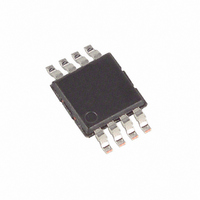
MAX145ACUA+ Maxim Integrated Products, MAX145ACUA+ Datasheet - Page 13

MAX145ACUA+
Manufacturer Part Number
MAX145ACUA+
Description
IC ADC 12BIT 108KSPS 8-UMAX
Manufacturer
Maxim Integrated Products
Datasheet
1.MAX144BEUA.pdf
(16 pages)
Specifications of MAX145ACUA+
Number Of Bits
12
Sampling Rate (per Second)
108k
Data Interface
MICROWIRE™, QSPI™, Serial, SPI™
Number Of Converters
1
Power Dissipation (max)
330mW
Voltage Supply Source
Single Supply
Operating Temperature
0°C ~ 70°C
Mounting Type
Surface Mount
Package / Case
8-TSSOP, 8-MSOP (0.118", 3.00mm Width)
Lead Free Status / RoHS Status
Lead free / RoHS Compliant
Table 3. Detailed SSPSTAT Register Contents
For best performance, use printed circuit boards
(PCBs). Wire-wrap configurations are not recommend-
ed, since the layout should ensure proper separation of
analog and digital traces. Run analog and digital lines
anti-parallel to each other, and don’t lay out digital sig-
nal paths underneath the ADC package. Use separate
analog and digital PCB ground sections with only one
star-point (Figure 11) connecting the two ground systems
X = Don’t care
Figure 10a. SPI Interface Connection for a PIC16/PIC17
Controller
Figure 10b. SPI Interface Timing with PIC16/PIC17 in Master Mode (CKE = 1, CKP = 0, SMP = 0, SSPM3–SSPM0 = 0001)
CS/SHDN
*WHEN CS/SHDN IS HIGH, DOUT = HIGH-Z
SMP
CKE
R/W
CONTROL BIT
D/A
DOUT*
UA
BF
P
S
SCLK
MAX144
MAX145
Layout, Grounding, and Bypassing
V
DD
CS/SHDN
BIT7
BIT6
BIT5
BIT4
BIT3
BIT2
BIT1
BIT0
DOUT
SCLK
GND
______________________________________________________________________________________
MAX144/MAX145
+2.7V, Low-Power, 2-Channel, 108ksps,
1
SAMPLING INSTANT
SETTINGS
2
0
1
X
X
X
X
X
X
3
CHID D11
1ST BYTE READ
SCK
SDI
I/O
4
Serial 12-Bit ADCs in 8-Pin µMAX
SPI Data Input Sample Phase. Input data is sampled at the middle of the data output
time.
SPI Clock Edge Select Bit. Data will be transmitted on the rising edge of the serial clock.
Data Address Bit
Stop Bit
Start Bit
Read/Write Bit Information
Update Address
Buffer Full Status Bit
MSB
PIC16/17
5
V
DD
D10
6
GND
SYNCHRONOUS SERIAL-PORT STATUS REGISTER (SSPSTAT)
D9
7
D8
8
(analog and digital). For lowest-noise operation, ensure
the ground return to the star ground’s power supply is
low impedance and as short as possible. Route digital
signals far away from sensitive analog and reference
inputs.
High-frequency noise in the power supply V
influence the proper operation of the ADC’s fast com-
parator. Bypass V
of two parallel capacitors (0.1µF and 1µF) located as
close as possible to the power supply pin of MAX144/
MAX145. Minimize capacitor lead length for best sup-
ply-noise rejection and add an attenuation resistor
(10Ω) if the power supply is extremely noisy.
D7
9
D6
10
DD
D5
11
to the star ground with a network
2ND BYTE READ
D4
12
D3
13
D2
14
D1
15
LSB
D0
16
DD
HIGH-Z
could
13


