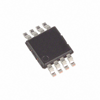
MAX145ACUA+ Maxim Integrated Products, MAX145ACUA+ Datasheet - Page 9

MAX145ACUA+
Manufacturer Part Number
MAX145ACUA+
Description
IC ADC 12BIT 108KSPS 8-UMAX
Manufacturer
Maxim Integrated Products
Datasheet
1.MAX144BEUA.pdf
(16 pages)
Specifications of MAX145ACUA+
Number Of Bits
12
Sampling Rate (per Second)
108k
Data Interface
MICROWIRE™, QSPI™, Serial, SPI™
Number Of Converters
1
Power Dissipation (max)
330mW
Voltage Supply Source
Single Supply
Operating Temperature
0°C ~ 70°C
Mounting Type
Surface Mount
Package / Case
8-TSSOP, 8-MSOP (0.118", 3.00mm Width)
Lead Free Status / RoHS Status
Lead free / RoHS Compliant
To start the conversion process on the MAX144/
MAX145, pull CS/SHDN low. At CS/SHDN’s falling
edge, the part wakes up and the internal T/H enters
track mode. In addition, the state of SCLK at
CS/SHDN’s falling edge selects internal (SCLK = high)
or external (SCLK = low) clock mode.
In internal clock mode, the MAX144/MAX145 run from
an internal, laser-trimmed oscillator to within 20% of the
2MHz specified clock rate. This releases the system
microprocessor from running the SAR conversion clock
and allows the conversion results to be read back at
the processor’s convenience, at any clock rate from 0
to 5MHz. Operating the MAX144/MAX145 in internal
clock mode is necessary for serial interfaces operating
with clock frequencies lower than 100kHz or greater
than 2.17MHz. Select internal clock mode (Figure 5), by
holding SCLK high during a high/low transition of
CS/SHDN. The first SCLK falling edge samples the data
and initiates a conversion using the integrated on-chip
oscillator. After the conversion, the oscillator shuts off
and DOUT goes high, signaling the end of conversion
(EOC). Data can then be read out with SCLK.
Figure 5. Internal Clock Mode Timing
Figure 6. External Clock Mode Timing
CS/SHDN
Internal Clock (f
DOUT
SCLK
ACTIVE
CS/SHDN
DOUT
SCLK
POWER
HIGH-Z
DOWN
ACTIVE
t
CS
_______________________________________________________________________________________
SCLK
ACTIVE
POWER
DOWN
+2.7V, Low-Power, 2-Channel, 108ksps,
HIGH-Z
t
CS
(t
t
WAKE
< 100kHz or f
ACQ
)
Selecting Clock Mode
ACTIVE
SAMPLING INSTANT
t
(t
WAKE
ACQ
)
Serial 12-Bit ADCs in 8-Pin µMAX
t
CONV
SAMPLING INSTANT
SCLK
1
2
> 2.17MHz)
3
CHID
EOC
4
1
MSB
1
5
2
D10
1
6
3
CHID
D9
7
The external clock mode (Figure 6) is selected by tran-
sitioning CS/SHDN from high to low while SCLK is low.
The external clock signal not only shifts data out, but
also drives the analog-to-digital conversion. The input
is sampled and conversion begins on the falling edge
of the second clock pulse. Conversion must be com-
pleted within 140µs to prevent degradation in the con-
version results caused by droop on the T/H capacitors.
External clock mode provides the best throughput for
clock frequencies between 100kHz and 2.17MHz.
Table 1 illustrates the 16-bit, serial data stream output
format for both the MAX144 and MAX145. The first
three bits are always logic high (including the EOC bit
for internal clock mode), followed by the channel identi-
fication (CHID = 0 for CH0, CHID = 1 for CH1, CHID = 0
for the MAX145), and then 12 bits of data in MSB-first
format. After the last bit has been read out, additional
SCLK pulses will clock out trailing zeros. DOUT transi-
tions on the falling edge of SCLK. The output remains
high-impedance when CS/SHDN is high.
4
MSB
D8
8
5
D10
D7
9
6
External Clock (f
D6
D9
10
7
D5
D8
11
8
D4
D7
12
9
D3
D6
13
10
D2
D5
14
11
SCLK
D1
D4
15
12
Output Data Format
D0
D3
16
13
ACTIVE
= 100kHz to 2.17MHz)
D2
14
HIGH-Z
D1
POWER
DOWN
15
D0
16
HIGH-Z
9


