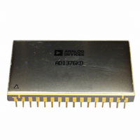
AD1377KD Analog Devices Inc, AD1377KD Datasheet - Page 8

AD1377KD
Manufacturer Part Number
AD1377KD
Description
IC ADC SNGL 16BIT 32-CDIP
Manufacturer
Analog Devices Inc
Datasheet
1.AD1376JD.pdf
(12 pages)
Specifications of AD1377KD
Data Interface
Parallel
Rohs Status
RoHS non-compliant
Number Of Bits
16
Sampling Rate (per Second)
111k
Number Of Converters
1
Power Dissipation (max)
800mW
Voltage Supply Source
Dual ±
Operating Temperature
0°C ~ 70°C
Mounting Type
Through Hole
Package / Case
32-DIP (0.900", 22.86)
Resolution (bits)
16bit
Sampling Rate
100kSPS
Input Channel Type
Single Ended
Supply Voltage Range - Digital
4.75V To 5.25V
Supply Current
-23mA
Digital Ic Case Style
DIP
Lead Free Status / RoHS Status
Contains lead / RoHS non-compliant
Available stocks
Company
Part Number
Manufacturer
Quantity
Price
AD1376/AD1377
Table 4. Input Scaling Connections
Input Signal Line
±10 V
±5 V
±2.5 V
0 V to +5 V
0 V to +10 V
0 V to +20 V
1
CALIBRATION (14-BIT RESOLUTION EXAMPLES)
External zero adjustment and gain adjustment potentiometers,
connected as shown in Figure 5 and Figure 6, are used for
device calibration. To prevent interaction of these two
adjustments, zero is always adjusted first and then gain. Zero is
adjusted with the analog input near the most negative end of the
analog range (0 for unipolar and minus full scale for bipolar
input ranges). Gain is adjusted with the analog input near the
most positive end of the analog range.
0 V to 10 V Range
Set analog input to +1 LSB
output = 11111111111110. Zero is now calibrated. Set analog
input to +FSR − 2 LSB = 9.99878 V. Adjust gain for
00000000000001 digital output code; full scale (gain) is now
calibrated. Half-scale calibration check: set analog input to
5.00000 V; digital output code should be 01111111111111.
−10 V to +10 V Range
Set analog input to −9.99878 V; adjust zero for 1111111111110
digital output (complementary offset binary) code. Set analog
input to 9.99756 V; adjust gain for 00000000000001 digital
output (complementary offset binary) code. Half-scale
calibration check: set analog input to 0.00000 V; digital output
(complementary offset binary) code should be 01111111111111.
Pin 27 is extremely sensitive to noise and should be guarded by ANALOG COMMON.
COMMON
BIPOLAR
COMP IN
ANALOG
OFFSET
25
24
27
26
22
Figure 10. Input Scaling Circuit
10V SPAN
20V SPAN
3.75kΩ
FROM DAC
7.5kΩ
R2
14
Output Code
COB
COB
COB
CSB
CSB
CSB
= 0.00061 V. Adjust zero for digital
R1
3.75kΩ
V
REF
COMPARATOR
Connect Pin 26 to
Pin 27
Pin 27
Pin 27
Pin 22
Pin 22
Pin 22
TO
SAR
1
1
1
Rev. D | Page 8 of 12
100kΩ
NOTE:
ANALOG (
100kΩ
NOTE:
ANALOG (
Other Ranges
Representative digital coding for 0 V to +10 V and −10 V to
+10 V ranges is given in the 0 V to 10 V Range section and
−10 V to +10 V Range section. Coding relationships and
calibration points for 0 V to +5 V, −2.5 V to +2.5 V, and −5 V to
+5 V ranges can be found by halving proportionally the
corresponding code equivalents listed for the 0 V to +10 V and
−10 V to +10 V ranges, respectively, as indicated in Table 5.
10kΩ
10kΩ
Connect Pin 24 to
Open
Input Signal
Open
Pin 27
Pin 27
Input Signal
TO
TO
+15V
–15V
+15V
–15V
+15V
–15V
+15V
–15V
0.01µF
0.01µF
GAIN
ADJ
GAIN
ADJ
300kΩ
300kΩ
1µF
1µF
1µF
1µF
) AND DIGITAL (
) AND DIGITAL (
1
1
+
+
+
+
29
28
22
21
29
28
22
21
Figure 11. Analog and Power Connections
Figure 12. Analog and Power Connections
+5V
+5V
for Bipolar −10 V to +10 V Input Range
for Unipolar 0 V to 10 V Input Range
) GROUNDS ARE NOT TIED INTERNALLY AND MUST BE CONNECTED EXTERNALLY
) GROUNDS ARE NOT TIED INTERNALLY AND MUST BE CONNECTED EXTERNALLY.
AD1376/
AD1377
AD1376/
AD1377
CONTROL
CONTROL
30
30
+
+
REF
1µF
REF
1µF
I
19
I
OS
OS
19
= 1.3mA
= 1.3mA
23
23
7.5kΩ
100kΩ
7.5kΩ
100kΩ
10kΩ
10kΩ
TO
TO
+15V
–15V
+15V
–15V
26
Connect Input Signal to
Pin 24
Pin 25
Pin 25
Pin 25
Pin 25
Pin 24
26
APPROMIXATION REGISTER
APPROMIXATION REGISTER
ZERO
ADJ
ZERO
ADJ
27
27
16-BIT SUCCESSIVE
16-BIT SUCCESSIVE
1.8MΩ
1.8MΩ
16-BIT DAC
16-BIT DAC
24
24
I
IN
25
I
25
IN
A
A
KEEP/
REJECT
KEEP/
REJECT
e
(–10V TO +10V)
e
(0V TO +10V)
IN
IN


