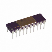
AD673JD Analog Devices Inc, AD673JD Datasheet - Page 3

AD673JD
Manufacturer Part Number
AD673JD
Description
IC ADC 8BIT W/REF/CLK/COMP 20DIP
Manufacturer
Analog Devices Inc
Datasheet
1.AD673JNZ.pdf
(8 pages)
Specifications of AD673JD
Rohs Status
RoHS non-compliant
Number Of Bits
8
Sampling Rate (per Second)
33k
Data Interface
Parallel
Number Of Converters
1
Voltage Supply Source
Dual ±
Operating Temperature
0°C ~ 70°C
Mounting Type
Through Hole
Package / Case
20-CDIP (0.300", 7.62mm)
Available stocks
Company
Part Number
Manufacturer
Quantity
Price
FUNCTIONAL DESCRIPTION
A block diagram of the AD673 is shown in Figure 1. The posi-
tive CONVERT pulse must be at least 500 ns wide. DR goes
high within 1.5 s after the leading edge of the convert pulse in-
dicating that the internal logic has been reset. The negative edge
of the CONVERT pulse initiates the conversion. The internal
8-bit current output DAC is sequenced by the integrated injec-
tion logic (I
most significant bit to least significant bit to provide an output
current which accurately balances the input signal current
through the 5 k resistor. The comparator determines whether
the addition of each successively weighted bit current causes the
DAC current sum to be greater or less than the input current; if
the sum is more, the bit is turned off. After testing all bits, the
SAR contains a 8-bit binary code which accurately represents
the input signal to within (0.05% of full scale).
The SAR drives DR low to indicate that the conversion is com-
plete and that the data is available to the output buffers. DATA
ENABLE can then be activated to enable the 8-bits of data de-
sired. DATA ENABLE should be brought high prior to the next
conversion to place the output buffers in the high impedance state.
REV. A
CONTROL
COMMON
BIPOLAR
ANALOG
ANALOG
OFFSET
READY
DATA
Figure 1. AD673 Functional Block Diagram
IN
2
L) successive approximation register (SAR) from its
COMP-
ARATOR
V+
5k
BURIED ZENER REF
V–
1
2
Model
AD673JN
AD673JD
AD673SD
AD673JP
NOTES
CURRENT
D = Ceramic DIP; N = Plastic DIP; P = Plastic Leaded Chip Carrier.
For details on grade and package offering screened in accordance with MIL-STD-883, refer to the
Analog Devices Military Products Databook .
OUTPUT
8-BIT
DAC
COMMON
DIGITAL
CLOCK
ABSOLUTE MAXIMUM RATINGS
V+ to Digital Common . . . . . . . . . . . . . . . . . . . . . 0 V to +7 V
V– to Digital Common . . . . . . . . . . . . . . . . . . . 0 V to –16.5 V
Analog Common to Digital Common . . . . . . . . . . . . . . .
Analog Input to Analog Common . . . . . . . . . . . . . . . . .
Control Inputs . . . . . . . . . . . . . . . . . . . . . . . . . . . . . . 0 V to V+
Digital Outputs (High Impedance State) . . . . . . . . . . 0 V to V+
Power Dissipation . . . . . . . . . . . . . . . . . . . . . . . . . . . . 800 mW
8-BIT
SAR
INT
2
CONVERT
AD673
Temperature
Range
0 C to +70 C
0 C to +70 C
–55 C to +125 C
0 C to +70 C
MSB
LSB
DB7
DB6
DB5
DB4
DB3
DB2
DB1
DB0
DATA
ENABLE
ORDERING GUIDE
–3–
Relative
Accuracy
The temperature compensated buried Zener reference provides
the primary voltage reference to the DAC and ensures excellent
stability with both time and temperature. The bipolar offset in-
put controls a switch which allows the positive bipolar offset
current (exactly equal to the value of the MSB less 1/2 LSB) to
be injected into the summing (+) node of the comparator to off-
set the DAC output. Thus the nominal 0 V to +10 V unipolar
input range becomes a –5 V to +5 V range. The 5 k thin-film
input resistor is trimmed so that with a full-scale input signal, an
input current will be generated which exactly matches the DAC
output with all bits on.
UNIPOLAR CONNECTION
The AD673 contains all the active components required to per-
form a complete A/D conversion. Thus, for many applications,
all that is necessary is connection of the power supplies (+5 V
and –12 V to –15 V), the analog input and the convert pulse.
However, there are some features and special connections which
should be considered for achieving optimum performance. The
functional pinout is shown in Figure 2.
The standard unipolar 0 V to +10 V range is obtained by short-
ing the bipolar offset control pin (Pin 16) to digital common
(Pin 17).
1/2 LSB max
1/2 LSB max
1/2 LSB max
1/2 LSB max
CONNECTED TO TEST POINTS AND SHOULD BE LEFT FLOATING
Figure 2. AD673 Pin Connections
Package Option
Plastic DIP (N-20)
Ceramic DIP (D-20)
Ceramic DIP (D-20)
PLCC (P-20A)
MSB DB7
LSB DB0
*
PINS 1 & 2 ARE INTERNALLY
DB1
DB2
DB3
DB4
DB5
DB6
NC
NC
*
*
15 V
10
1
2
3
4
5
6
7
8
9
1 V
(Not to Scale)
TOP VIEW
PIN 1
IDENTIFIER
AD673
1
20
19
18
17
16
15
14
13
12
11
DATA ENABLE
NC
DATA READY
DIGITAL COMMON
BIPOLAR OFFSET
ANALOG COMMON
ANALOG IN
V–
CONVERT
V+
AD673


