AD673JD Analog Devices Inc, AD673JD Datasheet - Page 6
AD673JD
Manufacturer Part Number
AD673JD
Description
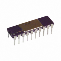
IC ADC 8BIT W/REF/CLK/COMP 20DIP
Manufacturer
Analog Devices Inc
Datasheet
1.AD673JNZ.pdf
(8 pages)
Specifications of AD673JD
Rohs Status
RoHS non-compliant
Number Of Bits
8
Sampling Rate (per Second)
33k
Data Interface
Parallel
Number Of Converters
1
Voltage Supply Source
Dual ±
Operating Temperature
0°C ~ 70°C
Mounting Type
Through Hole
Package / Case
20-CDIP (0.300", 7.62mm)
Available stocks
Company
Part Number
Manufacturer
Quantity
Price


AD673
GROUNDING CONSIDERATIONS
The AD673 provides separate Analog and Digital Common
connections. The circuit will operate properly with as much as
This permits more flexible control of system common bussing
and digital and analog returns.
In normal operation, the Analog Common terminal may gener-
ate transient currents of up to 2 mA during a conversion. In ad-
dition a static current of about 2 mA will flow into Analog
Common in the unipolar mode after a conversion is complete.
The Analog Common current will be modulated by the varia-
tions in input signal.
The absolute maximum voltage rating between the two com-
mons is 1 volt. It is recommended that a parallel pair of
back-to-back protection diodes be connected between the
commons if they are not connected locally.
CONTROL AND TIMING OF THE AD673
The operation of the AD673 is controlled by two inputs: CON-
VERT and DATA ENABLE.
Starting a Conversion
The conversion cycle is initiated by a positive-going CONVERT
pulse at least 500 ns wide. The rising edge of this pulse resets
the internal logic, clears the result of the previous conversion,
and sets DR high. The falling edge of CONVERT begins the
conversion cycle. When conversion is completed DR returns
low. During the conversion cycle, DE should be held high. If
DE goes low during a conversion, the data output buffers will be
enabled and intermediate conversion results will be present on
the data output pins. This may cause bus conflicts if other de-
vices in a system are trying to use the bus.
Reading the Data
The three-state data output buffers is enabled by DE. Access
time of these buffers is typically 150 ns (250 maximum). The
Data outputs remain valid until 50 ns after the enable signal re-
turns high, and are completely into the high-impedance state
100 ns later.
200 mV of common-mode voltage between the two commons.
CONVERT
DB0–DB7
DR
DE
V
IH
+ V
2
IMPEDANCE
IL
V
HIGH
IH
Figure 9. Convert Timing
Figure 10. Read Timing
+ V
2
t
CS
t
IL
DSC
V
V
t
DD
OH
OL
V
OH
VALID
DATA
+ V
2
OL
t
t
C
HD
t
HL
IMPEDANCE
HIGH
–6–
TIMING SPECIFICATIONS
Parameter
CONVERT Pulse Width
DR Delay from CONVERT t
Conversion Time
Data Access Time
Data Valid after DE High
Output Float Delay
MICROPROCESSOR INTERFACE CONSIDERATIONS—
GENERAL
When an analog-to-digital converter like the AD673 is inter-
faced to a microprocessor, several details of the interface must
be considered. First, a signal to start the converter must be gen-
erated; then an appropriate delay period must be allowed to pass
before valid conversion data may be read. In most applications,
the AD673 can interface to a microprocessor system with little
or no external logic.
The most popular control signal configuration consists of de-
coding the address assigned to the AD673, then gating this sig-
nal with the system’s WR signal to generate the CONVERT
pulse, and gating it with RD to enable the output buffers. The
use of a memory address and memory WR and RD signals de-
notes “memory-mapped” I/O interfacing, while the use of a
separate I/O address space denotes “isolated I/O” interfacing.
Figure 11 shows a generalized diagram of the control logic for
an AD673 interfaced to an 8-bit data bus, where an address
ADC ADDR has been decoded. ADC ADDR starts the con-
verter when written to (the actual data being written to the con-
verter does not matter) and contains the high byte data during
read operations.
Figure 11. General AD673 Interface to 8-Bit
Microprocessor
Symbol Min Typ Max Units
t
t
t
t
t
CS
DSC
C
DD
HD
HL
500 —
—
10
0
50
—
1
20
150 250
—
100 200
—
1.5
30
—
REV. A
ns
ns
ns
ns
s
s
Related parts for AD673JD
Image
Part Number
Description
Manufacturer
Datasheet
Request
R

Part Number:
Description:
±1.7g Dual-Axis IMEMS Accelerometer Evaluation Board
Manufacturer:
Analog Devices Inc
Datasheet:

Part Number:
Description:
Inertial Sensor Evaluation System
Manufacturer:
Analog Devices Inc
Datasheet:
Part Number:
Description:
Manufacturer:
Analog Devices Inc
Datasheet:
Part Number:
Description:
Manufacturer:
Analog Devices Inc
Datasheet:
Part Number:
Description:
Manufacturer:
Analog Devices Inc
Datasheet:
Part Number:
Description:
Manufacturer:
Analog Devices Inc
Datasheet:
Part Number:
Description:
Manufacturer:
Analog Devices Inc
Datasheet:
Part Number:
Description:
Manufacturer:
Analog Devices Inc
Datasheet:
Part Number:
Description:
Manufacturer:
Analog Devices Inc
Datasheet:
Part Number:
Description:
Manufacturer:
Analog Devices Inc
Datasheet:
Part Number:
Description:
Manufacturer:
Analog Devices Inc
Datasheet:
Part Number:
Description:
Manufacturer:
Analog Devices Inc
Datasheet:
Part Number:
Description:
Manufacturer:
Analog Devices Inc
Datasheet: