AD673JD Analog Devices Inc, AD673JD Datasheet - Page 5
AD673JD
Manufacturer Part Number
AD673JD
Description
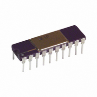
IC ADC 8BIT W/REF/CLK/COMP 20DIP
Manufacturer
Analog Devices Inc
Datasheet
1.AD673JNZ.pdf
(8 pages)
Specifications of AD673JD
Rohs Status
RoHS non-compliant
Number Of Bits
8
Sampling Rate (per Second)
33k
Data Interface
Parallel
Number Of Converters
1
Voltage Supply Source
Dual ±
Operating Temperature
0°C ~ 70°C
Mounting Type
Through Hole
Package / Case
20-CDIP (0.300", 7.62mm)
Available stocks
Company
Part Number
Manufacturer
Quantity
Price


BIPOLAR CONNECTION
To obtain the bipolar –5 V to +5 V range with an offset binary
output code, the bipolar offset control pin is left open.
A –5.00 volt signal will give a 8-bit code of 00000000; an input
of 0.00 volts results in an output code of 10000000 and +4.961
volts at the input yields the 11111111 code. The nominal trans-
fer curve is shown in Figure 6.
Note that in the bipolar mode, the code transitions are offset
1/4 LSB such that an input voltage of 0 volts –5 mV to +35 mV
yields the code representing zero (10000000). Each output code
is then centered on its nominal input voltage.
Full-Scale Calibration
Full-Scale Calibration is accomplished in the same manner as in
Unipolar operation except the full-scale input voltage is +4.61
volts.
Negative Full-Scale Calibration
The circuit in Figure 4a can also be used in Bipolar operation to
offset the input voltage (nominally –5 V) which results in the
000000 00 code. R2 should be omitted to obtain a symmetrical
range.
The bipolar offset control input is not directly TTL compatible
but a TTL interface for logic control can be constructed as
shown in Figure 7.
REV. A
Figure 7. Bipolar Offset Controlled by Logic Gate
Gate Output = 1 Unipolar 0 V–10 V Input Range
Gate Output = 0 Bipolar 5 V Input Range
Figure 6. AD673 Transfer Curve—Bipolar Operation
–5–
SAMPLE-HOLD AMPLIFIER CONNECTION
TO THE AD673
Many situations in high-speed acquisition systems or digitizing
rapidly changing signals require a sample-hold amplifier (SHA)
in front of the A-D converter. The SHA can acquire and hold a
signal faster than the converter can perform a conversion. A
SHA can also be used to accurately define the exact point in
time at which the signal is sampled. For the AD673, a SHA can
also serve as a high input impedance buffer.
Figure 8 shows the AD673 connected to the AD582 monolithic
SHA for high speed signal acquisition. In this configuration, the
AD582 will acquire a 10 volt signal in less than 10 s with a
droop rate less than 100 V/ms.
DR goes high after the conversion is initiated to indicate that re-
set of the SAR is complete. In Figure 8 it is also used to put the
AD582 into the hold mode while the AD673 begins its conver-
sion cycle. (The AD582 settles to final value well in advance of
the first comparator decision inside the AD673).
DR goes low when the conversion is complete placing the
AD582 back in the sample mode. Configured as shown in Fig-
ure 8, the next conversion can be initiated after a 10 s delay to
allow for signal acquisition by the AD582.
Observe carefully the ground, supply, and bypass capacitor con-
nections between the two devices. This will minimize ground
noise and interference during the conversion cycle.
Figure 8. Sample-Hold Interface to the AD673
AD673
Related parts for AD673JD
Image
Part Number
Description
Manufacturer
Datasheet
Request
R

Part Number:
Description:
±1.7g Dual-Axis IMEMS Accelerometer Evaluation Board
Manufacturer:
Analog Devices Inc
Datasheet:

Part Number:
Description:
Inertial Sensor Evaluation System
Manufacturer:
Analog Devices Inc
Datasheet:
Part Number:
Description:
Manufacturer:
Analog Devices Inc
Datasheet:
Part Number:
Description:
Manufacturer:
Analog Devices Inc
Datasheet:
Part Number:
Description:
Manufacturer:
Analog Devices Inc
Datasheet:
Part Number:
Description:
Manufacturer:
Analog Devices Inc
Datasheet:
Part Number:
Description:
Manufacturer:
Analog Devices Inc
Datasheet:
Part Number:
Description:
Manufacturer:
Analog Devices Inc
Datasheet:
Part Number:
Description:
Manufacturer:
Analog Devices Inc
Datasheet:
Part Number:
Description:
Manufacturer:
Analog Devices Inc
Datasheet:
Part Number:
Description:
Manufacturer:
Analog Devices Inc
Datasheet:
Part Number:
Description:
Manufacturer:
Analog Devices Inc
Datasheet:
Part Number:
Description:
Manufacturer:
Analog Devices Inc
Datasheet: