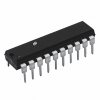
ADC08161CIN National Semiconductor, ADC08161CIN Datasheet

ADC08161CIN
Specifications of ADC08161CIN
Related parts for ADC08161CIN
ADC08161CIN Summary of contents
Page 1
... For ease of interface to microprocessors, this part has been designed to appear as a memory location or I/O port without the need for external interfacing logic. Block Diagram TRI-STATE ® registered trademark of National Semiconductor Corporation. © 1997 National Semiconductor Corporation DS011149 Key Specifications n Resolution: 8 Bits ...
Page 2
... REF− 25˚C. ; all other limits T MAX A J Conditions = 5V V REF ADC08161BIN, BIWM ADC08161CIN, CIWM = 5V V REF ADC08161BIN, BIWM ADC08161CIN, CIWM, = 2.5V, All Suffixes V REF = 2.5V V REF ADC08161, All Suffixes = 5V V REF = 2.5V V REF (Note 10) On Channel Input = 5V, Off Channel Input = 0V ...
Page 3
... IN p kHz 4. p kHz ns 5V unless otherwise specified. Boldface r f REF+ REF− 25˚ ADC08161BIN, ADC08161CIN, Conditions + Mode Pin Figures Mode Pin Figure 2 ) Mode Pin to GND ( Figure Mode Pin Figure 2 ) Mode Pin to GND, ( Figure 100 pF, Mode Pin to GND L ( Figure 100 Mode Pin to V ...
Page 4
... ADC08161BIN, ADC08161CIN, ADC08161BIWM, ADC08161CIWM Typical (Note 5 4. 0.005 = 0V L −0.005 + = 4.75V = −360 µA OUT = −10 µA OUT + = 4.75V = 1.6 mA OUT = 5.0V OUT = 0V OUT = 0V OUT 4 ADC08161BIN, ADC08161CIN, ADC08161BIWM, Units ADC08161CIWM (Limit) Typical Limit (Note 7) (Note (max) 60 115 ns (max (min (max (max MIN ...
Page 5
... An absolute analog input signal voltage range plied 4.950V over temperature variations, initial tolerance, and loading. (Continued unless otherwise specified. Boldface limits apply for T Conditions ADC08161BIN, ADC08161CIN, ADC08161BIWM, ADC08161CIWM Typical (Note OUT 11 unless otherwise specified. Boldface limits apply for T Conditions “ ...
Page 6
Bandgap Reference Electrical Characteristics Note 11: Off-channel leakage current is measured on the on-channel selection. TRI-STATE Test Circuit and Waveforms www.national.com (Continued) DS011149 DS011149 FIGURE 1. ...
Page 7
TRI-STATE Test Circuit and Waveforms FIGURE 2. WR -RD Mode with t FIGURE 3. WR -RD Mode with t (Continued) t (Mode Pin is High) RD INTL > t (Mode Pin is High) RD INTL 7 DS011149-7 DS011149-8 www.national.com ...
Page 8
TRI-STATE Test Circuit and Waveforms FIGURE 4. WR -RD Mode Reduced Interface System Connection with (Mode Pin is High) FIGURE 5. RD Mode (Pipeline Operation); t Typical Performance Characteristics t vs Temperature CRD DS011149-23 www.national.com ...
Page 9
... Typical Performance Characteristics Supply Current vs Temperature DS011149-26 Connection Diagram See NS Package Number N20A or M20A Ordering Information Industrial (−40˚C T 85˚C) A ADC08161BIN, ADC08161CIN ADC08161BIWM, ADC08161CIWM (Continued) Logic Threshold vs Reference Output Voltage vs Temperature Temperature DS011149-27 Output Current vs Temperature DS011149-29 Dual-In-Line and Wide-Body ...
Page 10
Pin Description (Continued) WR /RDY WR -RD Mode (Logic high applied to MODE pin With CS low, the conversion is started on the rising edge The digital result will be strobed into the output latch ...
Page 11
Application Information FIGURE 6. Block Diagram of the ADC08161 Multi-Step Flash Architecture 1.0 FUNCTIONAL DESCRIPTION The ADC08161 performs an 8-bit analog-to-digital conver- sion using a multi-step flash technique. The first flash gener- ates the five most significant bits (MSBs) and ...
Page 12
Application Information points are then connected to the eight flash comparators. For example, if the analog input signal applied tween 0 and 3/ REF REF REF+ mator decoder instructs the comparator multiplexer to ...
Page 13
Application Information (Continued) The voltage at V sets the input level that produces a REF− digital output of all zeroes. Through V is not itself differen- IN tial, the reference design affords nearly differential-input ca- pability for some measurement applications. ...
Page 14
Application Information Internal Reference 2.5V Full-Scale (Standard Application) DS011149-19 Note: Bypass capacitors consist of a 0.1 µF ceramic in parallel with a 10 µF bead tantalum, unless otherwise specified. FIGURE 9. Typical Connection. Note the multiple bypass capacitors on the ...
Page 15
... Physical Dimensions inches (millimeters) unless otherwise noted Order Number ADC08161BIWM or ADC08161CIWM Order Number ADC08161BIN or ADC08161CIN Wide-Body Small-Outline NS Package Number M20B Dual-In-Line NS Package Number N20A 15 www.national.com ...
Page 16
... National Semiconductor Asia Pacific Customer Fax: +49 (0) 1 80-530 85 86 Response Group Email: europe.support@nsc.com Tel: 65-2544466 Fax: 65-2504466 Tel: +49 (0) 1 80-532 78 32 Email: sea.support@nsc.com Tel: +49 (0) 1 80-534 16 80 National Semiconductor Japan Ltd. Tel: 81-3-5620-6175 Fax: 81-3-5620-6179 ...


