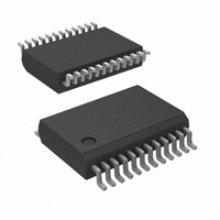
ADC12H034CIMSAX/NOPB National Semiconductor, ADC12H034CIMSAX/NOPB Datasheet - Page 35

ADC12H034CIMSAX/NOPB
Manufacturer Part Number
ADC12H034CIMSAX/NOPB
Description
ADC 12BIT W/S&H +SIGN 24-SSOP
Manufacturer
National Semiconductor
Datasheet
1.ADC12030CIWMNOPB.pdf
(42 pages)
Specifications of ADC12H034CIMSAX/NOPB
Number Of Bits
12
Data Interface
NSC MICROWIRE™, Serial
Number Of Converters
4
Power Dissipation (max)
33mW
Voltage Supply Source
Analog and Digital
Operating Temperature
-40°C ~ 85°C
Mounting Type
Surface Mount
Package / Case
24-SSOP (0.200", 5.30mm Width)
Lead Free Status / RoHS Status
Lead free / RoHS Compliant
Other names
ADC12H034CIMSAX
4.0 ANALOG INPUT VOLTAGE RANGE
The ADC12030/2/4/8's fully differential ADC generate a two's
complement output that is found by using the equations
shown below:
Round off to the nearest integer value between −4096 to 4095
for 12-bit resolution and between −256 to 255 for 8-bit reso-
lution if the result of the above equation is not a whole number.
Examples are shown in the table below:
5.0 INPUT CURRENT
At the start of the acquisition window (t
flows into or out of the analog input pins (A/DIN1 and A/DIN2)
depending upon the input voltage polarity. The analog input
pins are CH0–CH7 and COM when A/DIN1 is tied to MUX-
OUT1 and A/DIN2 is tied to MUXOUT2. The peak value of
this input current will depend upon the actual input voltage
applied, the source impedance and the internal multiplexer
switch on resistance. With MUXOUT1 tied to A/DIN1 and
MUXOUT2 tied to A/DIN2 the internal multiplexer switch on
resistance is typically 1.6 kΩ. The A/DIN1 and A/DIN2 mux
on resistance is typically 750Ω.
+4.096V
+4.096V
+4.096V
for (12-bit) resolution the Output Code =
for (8-bit) resolution the Output Code =
+2.5V
V
REF
+
FIGURE 17. V
V
+1V
0V
0V
0V
REF
−
+2.499V +2.500V 1,1111,1111,1111
+1.5V
V
+3V
0V
IN
+
REF
+4.096V 1,0000,0000,0000
Operating Range
V
0V
0V
IN
−
A
) a charging current
0,1111,1111,1111
0,1011,1011,1000
Digital Output
Code
1135445
35
6.0 INPUT SOURCE RESISTANCE
For low impedance voltage sources (<600Ω), the input charg-
ing current will decay before the end of the S/H's acquisition
time of 2 µs (10 CCLK periods with f
that will not introduce any conversion errors. For high source
impedances, the S/H's acquisition time can be increased to
18 or 34 CCLK periods. For less ADC resolution and/or slower
CCLK frequencies the S/H's acquisition time may be de-
creased to 6 CCLK periods. To determine the number of clock
periods (N
source impedance for the various resolutions the following
equations can be used:
Where f
and R
ple, operating with a resolution of 12 Bits+sign, a 5 MHz clock
frequency and maximum acquisition time of 34 conversion
clock periods the ADC's analog inputs can handle a source
impedance as high as 6 kΩ. The acquisition time may also be
extended to compensate for the settling or response time of
external circuitry connected between the MUXOUT and
A/DIN pins.
An acquisition starts at a falling edge of SCLK and ends at a
rising edge of CCLK (see timing diagrams). If SCLK and
CCLK are asynchronous, one extra CCLK clock period may
be inserted into the programmed acquisition time for synchro-
nization. Therefore, with asynchronous SCLK and CCLKs the
acquisition time will change from conversion to conversion.
7.0 INPUT BYPASS CAPACITANCE
External capacitors (0.01 µF–0.1 µF) can be connected be-
tween the analog input pins, CH0–CH7, and analog ground
to filter any noise caused by inductive pickup associated with
long input leads. These capacitors will not degrade the con-
version accuracy.
8.0 NOISE
The leads to each of the analog multiplexer input pins should
be kept as short as possible. This will minimize input noise
and clock frequency coupling that can cause conversion er-
rors. Input filtering can be used to reduce the effects of the
noise sources.
9.0 POWER SUPPLIES
Noise spikes on the V
version errors; the comparator will respond to the noise. The
ADC is especially sensitive to any power supply spikes that
occur during the Auto Zero or linearity correction. The mini-
mum power supply bypassing capacitors recommended are
low inductance tantalum capacitors of 10 µF or greater par-
alleled with 0.1 µF monolithic ceramic capacitors. More or
different bypassing may be necessary depending upon the
overall system requirements. Separate bypass capacitors
should be used for the V
close as possible to these pins.
10.0 GROUNDING
The ADC12030/2/4/8's performance can be maximized
through proper grounding techniques. These include the use
of separate analog and digital areas of the board with analog
and digital components and traces located only in their re-
spective areas. Bypass capacitors of 0.01 µF and 0.1 µF
surface mount capacitors and a 10 µF are recommended at
each of the power supply pins for best performance. These
12 Bit + Sign N
8 Bit + Sign N
S
is the external source resistance in kΩ. As an exam-
C
is the conversion clock (CCLK) frequency in MHz
c
) required for the acquisition time with a specific
C
C
= [R
= [R
A
+
and V
S
S
A
+
+ 2.3] × f
+ 2.3] × f
and V
D
+
supply lines can cause con-
D
+
C
C
supplies and placed as
C
× 0.824
× 0.57
= 5 MHz), to a value
www.national.com


