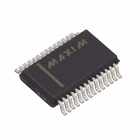
MAX1414CAI+ Maxim Integrated Products, MAX1414CAI+ Datasheet - Page 35

MAX1414CAI+
Manufacturer Part Number
MAX1414CAI+
Description
IC DAS 16BIT LP 28-SSOP
Manufacturer
Maxim Integrated Products
Type
Data Acquisition System (DAS)r
Datasheet
1.MAX1409CAP.pdf
(48 pages)
Specifications of MAX1414CAI+
Resolution (bits)
16 b
Sampling Rate (per Second)
60
Data Interface
Serial
Voltage Supply Source
Analog and Digital
Voltage - Supply
2.7 V ~ 3.6 V
Operating Temperature
0°C ~ 70°C
Mounting Type
Surface Mount
Package / Case
28-SSOP
Number Of Converters
1
Resolution
16 bit
Interface Type
Serial (4-Wire, SPI, QSPI, Microwire)
Supply Voltage (max)
3.6 V
Supply Voltage (min)
2.7 V
Maximum Power Dissipation
762 mW
Maximum Operating Temperature
+ 70 C
Mounting Style
SMD/SMT
Minimum Operating Temperature
0 C
Lead Free Status / RoHS Status
Lead free / RoHS Compliant
Table 8 shows the bit values of some key registers in
different power modes under various conditions. Use
REFE: Internal Reference Power Enable. When REFE is
set to 1, the internal reference is powered up. When
REFE is set to 0, the internal reference is powered down
allowing an external reference to be connected to REF.
ADCE: ADC Power Enable. When ADCE is set to 1, the
ADC is powered up. When ADCE is set to 0, the ADC is
powered down.
Table 8. Related Bit Values During Specified Mode
N/A: Programming the part into these modes would not alter the content of the corresponding bit.
32kHz Oscillator
RTC
Low V
Monitor (2.7V)
RESET Voltage
Monitor (1.8V)
Reset Bit
Low V
Voltage-Monitor
Threshold Selection
Bias Circuit
PLL
PLL Output
SHDN Output
DAC1
DAC2
ADC MUX
Bandgap Reference
Signal-Detect
Comparator
ADC Buffers
ADC
NAME
DEFAULT
CIRCUIT BLOCK
DD
DD
Voltage
Status Bit
FIRST BIT (MSB)
Low-Power, 16-Bit Multichannel DAS with
Internal Reference,10-Bit DACs, and RTC
REFE
______________________________________________________________________________________
0
BIASE
MUX
ADC
SHDE
DA1E
DA2E
SDCE
BUFE
LVDE
LSDE
REFE
PLLE
PLLE
LVD
RST
BIT
CH
CH
VM
Power-Control Registers
INITIAL POWER-UP
1 (FOUT is enabled)
1 (RESET asserted)
1 ( S HD N p i n = hi g h)
ADCE
0 (oscillator is on)
1 (2.7V monitor is
0 (1.8V monitor is
Biase = 1 (biase
0 (select 2.7V)
0
0 (RTC is on)
1 (PLL is on)
circuit is on)
1 (low V
on)
off)
0
0
0
0
0
0
0
DD
)
BUFE
0
1 if VM = 0
0 if VM = 1
0 if VM = 0
1 if VM = 1
SLEEP
N/A
N/A
N/A
N/A
N/A
0
0
0
0
0
0
0
0
0
0
0
MUXE
0
this as a quick reference when programming the
MAX1407/MAX1408/MAX1409/MAX1414 family.
BUFE: ADC Input Buffer Power Enable. A logic 1
enables the power-up of the ADC input buffers, while a
logic 0 powers-down the buffers.
MUXE: Multiplexer enable. A logic 0 disables the multi-
plexer outputs while a logic 1 enables them.
STANDBY
0 if VM = 0
1 if VM = 1
N/A
N/A
N/A
N/A
N/A
1
1
1
1
1
0
0
0
0
0
0
0
DA1E
0
0 if VM = 0
1 if VM = 1
IDLE
N/A
N/A
N/A
N/A
N/A
1
1
1
1
1
1
1
1
1
1
0
0
DA2E
0
POWER1 REGISTER (11000)
0 if VM = 0
1 if VM = 1
RUN
N/A
N/A
N/A
N/A
N/A
1
1
1
1
1
1
1
1
1
1
1
1
—
0
WAKE-UP EVENT
N/A
N/A
N/A
N/A
N/A
N/A
N/A
N/A
N/A
N/A
N/A
N/A
N/A
1
1
1
1
1
(LSB)
—
0
35


