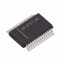
MAX1414CAI+ Maxim Integrated Products, MAX1414CAI+ Datasheet - Page 7

MAX1414CAI+
Manufacturer Part Number
MAX1414CAI+
Description
IC DAS 16BIT LP 28-SSOP
Manufacturer
Maxim Integrated Products
Type
Data Acquisition System (DAS)r
Datasheet
1.MAX1409CAP.pdf
(48 pages)
Specifications of MAX1414CAI+
Resolution (bits)
16 b
Sampling Rate (per Second)
60
Data Interface
Serial
Voltage Supply Source
Analog and Digital
Voltage - Supply
2.7 V ~ 3.6 V
Operating Temperature
0°C ~ 70°C
Mounting Type
Surface Mount
Package / Case
28-SSOP
Number Of Converters
1
Resolution
16 bit
Interface Type
Serial (4-Wire, SPI, QSPI, Microwire)
Supply Voltage (max)
3.6 V
Supply Voltage (min)
2.7 V
Maximum Power Dissipation
762 mW
Maximum Operating Temperature
+ 70 C
Mounting Style
SMD/SMT
Minimum Operating Temperature
0 C
Lead Free Status / RoHS Status
Lead free / RoHS Compliant
TIMING CHARACTERISTICS (continued)
(MAX1407/MAX1408/MAX1409/MAX1414: AV
Note 1: Single conversion.
Note 2: DNL and INL are measured between code 010hex and 3FFhex.
Note 3: Offset error is referenced to code 010hex.
Note 4: Output swing is a function of external gain-setting feedback resistors and REF voltage.
Note 5: Measured with no load on FOUT, DOUT, and the DAC amplifiers. SCLK is idle, and all digital inputs are at DGND or DV
Note 6: SHDN stays high if the PLL is on.
Note 7: Actual worst-case performance is ±2.5LSB. Guaranteed limit of ±3.5LSB is due to production test limitation.
Note 8: Guaranteed by design. Not production tested.
TYPICAL TIMING PARAMETERS
OUT1/OUT2 Turn-Off Time
Sleep Voltage Monitor Timeout
Period
WU1 or WU2 Pulse Width
Shutdown Deassert Delay
FOUT Turn-On Time
INT Delay
FOUT Disable Delay
SHDN Assertion Delay
PARAMETER
Low-Power, 16-Bit Multichannel DAS with
Internal Reference,10-Bit DACs, and RTC
_______________________________________________________________________________________
SYMBOL
t
t
t
DFON
t
DFOF
t
DSLP
t
t
DPU
DPD
WU
DFI
DD
= DV
Input impedance > 1MΩ
(MAX1407/MAX1409/MAX1414 only)
The delay for the sleep voltage monitor
output, RESET, to go high after AV
above the reset threshold (+1.8V when bit
VM = 1 and +2.7V, when bit VM = 0); this is
largely driven by the startup of the 32kHz
oscillator
Minimum pulse width required to detect a
wake-up event
The delay for SHDN to go high after a valid
wake-up event
The turn-on time for the high-frequency
clock; it is gated by an AND function with
three signals—the RESET signal, the internal
low voltage V
assertion of the PLL; the time delay is timed
from when the low-voltage monitor trips or
the RESET going high, whichever happens
later; FOUT always starts in the low state
The delay for INT to go low after the FOUT
clock output has been enabled; INT is used
as an interrupt signal to inform the µP the
high-frequency clock has started
The delay after a shutdown command has
asserted and before FOUT is disabled; this
gives the microcontroller time to clean up
and go into Sleep mode properly
The delay after a shutdown command has
asserted and before SHDN is pulled low
(turning off the DC-DC converter) (Note 6)
DD
= 2.7V to 3.6V, T
DD
CONDITIONS
monitor signal, and the
A
= T
MIN
to T
DD
MAX,
rises
unless otherwise noted.)
MIN
31.25
TYP
1.54
7.82
1.95
2.93
100
1
1
MAX
UNITS
ms
ms
ms
ms
DD
µs
µs
µs
s
.
7


