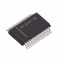
MAX1414CAI+ Maxim Integrated Products, MAX1414CAI+ Datasheet - Page 37

MAX1414CAI+
Manufacturer Part Number
MAX1414CAI+
Description
IC DAS 16BIT LP 28-SSOP
Manufacturer
Maxim Integrated Products
Type
Data Acquisition System (DAS)r
Datasheet
1.MAX1409CAP.pdf
(48 pages)
Specifications of MAX1414CAI+
Resolution (bits)
16 b
Sampling Rate (per Second)
60
Data Interface
Serial
Voltage Supply Source
Analog and Digital
Voltage - Supply
2.7 V ~ 3.6 V
Operating Temperature
0°C ~ 70°C
Mounting Type
Surface Mount
Package / Case
28-SSOP
Number Of Converters
1
Resolution
16 bit
Interface Type
Serial (4-Wire, SPI, QSPI, Microwire)
Supply Voltage (max)
3.6 V
Supply Voltage (min)
2.7 V
Maximum Power Dissipation
762 mW
Maximum Operating Temperature
+ 70 C
Mounting Style
SMD/SMT
Minimum Operating Temperature
0 C
Lead Free Status / RoHS Status
Lead free / RoHS Compliant
Three write operations are needed for every update of
the ALARM and RTC registers. First set the WE bit of
the Alarm/Clock_CTRL Register to 1. Update the Alarm,
RTC, and Alarm/Clock_CTRL Register with the new val-
ues, and then set the WE bit back to 0. This will avoid
collisions in setting the time.
At initial power-up, the MAX1407/MAX1408/MAX1409/
MAX1414 are in Standby mode. Figure 15 illustrates the
timing of various signals during initial Power-Up, Sleep
mode, and Wake-Up. t
RESET goes high. t
is enabled. INT is enabled to t
enabled.
The MAX1407/MAX1408/MAX1409/MAX1414 have fou
distinct power modes, Sleep mode, Standby mode, Idle
mode, and Run mode. Table 9 lists the power-on status
of the various blocks of the MAX1407/MAX1408/
MAX1409/MAX1414. Each individual circuit block can
be powered up through the serial interface by writing to
the appropriate power registers.
In Sleep mode, only the crystal oscillator, RTC, data
registers, wake-up circuitry, and RESET Voltage
Monitor are powered up. Sleep mode is entered by
addressing the Sleep register through the serial inter-
face. Sleep mode preserves any data in the data regis-
ters. To exit Sleep mode, pull either WU1 or WU2 low or
address other Power mode registers (Standby, Idle,
Run, Power1, or Power2 registers). Asserting WU1 or
WU2 or the occurence of a Time of Day Alarm while in
Sleep mode places the device in Standby mode.
After initial power-up or after exiting Sleep mode
through a wake-up event, the MAX1407/MAX1408/
MAX1409/MAX1414 are in Standby mode. Standby
mode can also be entered by addressing the Standby
register. In Standby mode, SHDN is high, FOUT is
enabled, the Low V
powered up, and INT is low. INT will return to a logic
high after the µP begins writing to any register through
the serial interface (once a start bit is detected through
the serial interface).
Applications Information
Low-Power, 16-Bit Multichannel DAS with
Internal Reference,10-Bit DACs, and RTC
Power-On Reset or Power-Up
Alarm and RTC Programming
______________________________________________________________________________________
DFON
DD
DSLP
voltage monitor and the PLL are
after RESET goes high, FOUT
after AV
DFI
DD
Power Modes
exceeds +2.7V,
after FOUT is
Standby Mode
Sleep Mode
In Idle mode, only the ADC and ADC input buffers are
shutdown. All the other blocks are powered up. Enter
Idle mode by addressing the Idle register.
In Run mode, all the functional blocks are powered up
and the ADC is ready to start conversion. Enter Run
mode by either writing to the Run register or by individu-
ally powering up each circuit through the serial interface.
Wake-Up mode is entered whenever a wake-up event,
such as an assertion of WU1 or WU2 or a time-of-day
alarm occurs. The Low V
enabled, and SHDN goes high. Different from the
Standby mode, the status of the other power blocks
remains unchanged.
The digital filter does not provide any rejection close to
the harmonics of the modulator sample frequency.
However, due to the high oversampling ratio of the
MAX1407/MAX1408/MAX1409/MAX1414, these bands
occupy only a small fraction of the spectrum and most
broadband noise is filtered. Therefore, the analog filter-
ing requirements in front of the MAX1407/MAX1408/
MAX1409/MAX1414 are considerably reduced com-
pared to a conventional converter with no on-chip filter-
ing. In addition, because the part’s common-mode
rejection of 90dB extends out to several kHz, common-
mode noise susceptibility in this frequency range is
substantially reduced.
Depending on the application, it may be necessary to
provide filtering prior to the MAX1407/MAX1408/
MAX1409/MAX1414 to eliminate unwanted frequencies
the digital filter does not reject. It may also be necessary
in some applications to provide additional filtering to
ensure that differential noise signals outside the frequen-
cy band of interest do not saturate the analog modulator.
If passive components are placed in front of the
MAX1407/MAX1408/MAX1409/MAX1414 when the part
is used in unbuffered mode, ensure that the source
impedance is low enough not to introduce gain errors in
the system. This can significantly limit the amount of
passive anti-aliasing filtering that can be applied in
front of the MAX1407/MAX1408/MAX1409/MAX1414 in
unbuffered mode. However, when the part is used in
buffered mode, large source impedances will simply
result in a small DC offset error (a 1kΩ source resis-
tance will cause an offset error of less than 0.5µV).
Therefore, where significant source impedances are
required, operate the device in buffered mode.
DD
monitor, PLL, FOUT are
Analog Filtering
Wake-Up
Run Mode
Idle Mode
37


