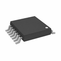
AD5292BRUZ-20 Analog Devices Inc, AD5292BRUZ-20 Datasheet - Page 11

AD5292BRUZ-20
Manufacturer Part Number
AD5292BRUZ-20
Description
IC POT DIG 1024P SPI 20K 14TSSOP
Manufacturer
Analog Devices Inc
Datasheet
1.AD5291BRUZ-20.pdf
(32 pages)
Specifications of AD5292BRUZ-20
Memory Type
Non-Volatile
Temperature Coefficient
35 ppm/°C Typical
Design Resources
30 V Low Cost DAC Using AD5292 Digital Potentiometer (CN0111) Variable Gain Noninverting Amplifier Using AD5292 and OP184 (CN0112) Variable Gain Inverting Amplifier Using AD5292 and OP184 (CN0113) Low Cost, High Voltage, Programmable Gain Instrumentation Amplifier Using AD5292 and AD8221 (CN0114) Programmable High Voltage Source with Boosted Output Current Using AD5292, OP184, and MOSFETs (CN0115) Programmable Bidirectional Current Source Using AD5292 and ADA4091-4 (CN0117) Logarithmic Audio Volume Control with Glitch Reduction Using AD5292 (CN0120)
Taps
1024
Resistance (ohms)
20K
Number Of Circuits
1
Interface
SPI Serial
Voltage - Supply
9 V ~ 33 V, ±9 V ~ 16.5 V
Operating Temperature
-40°C ~ 105°C
Mounting Type
Surface Mount
Package / Case
14-TSSOP
Resistance In Ohms
20K
End To End Resistance
20kohm
Resistance Tolerance
± 1%
No. Of Steps
1024
Control Interface
Serial, SPI
No. Of Pots
Single
Supply Voltage Range
± 9V To ± 16.5V
Rohs Compliant
Yes
Lead Free Status / RoHS Status
Lead free / RoHS Compliant
Other names
AD5292BRUZ-20-U1
AD5292BRUZ-20-U1
AD5292BRUZ-20-U1
Available stocks
Company
Part Number
Manufacturer
Quantity
Price
Company:
Part Number:
AD5292BRUZ-20
Manufacturer:
Micrel
Quantity:
100
Part Number:
AD5292BRUZ-20
Manufacturer:
ADI/亚德诺
Quantity:
20 000
PIN CONFIGURATION AND FUNCTION DESCRIPTIONS
Table 10. Pin Function Descriptions
Pin No.
1
2
3
4
5
6
7
8
9
10
11
12
13
14
Mnemonic
RESET
V
A
W
B
V
EXT_CAP
V
GND
DIN
SCLK
SYNC
SDO
RDY
SS
DD
LOGIC
Description
Hardware Reset Pin. Refreshes the RDAC register with the contents of the 20-TP memory register. Factory
default loads midscale until the first 20-TP wiper memory location is programmed. RESET is activated at the
logic high transition. Tie RESET to V
Negative Supply. Connect to 0 V for single-supply applications. This pin should be decoupled with 0.1 μF
ceramic capacitors and 10 μF capacitors.
Terminal A of RDAC. V
Wiper Terminal of RDAC. V
Terminal B of RDAC. V
Positive Power Supply. This pin should be decoupled with 0.1 μF ceramic capacitors and 10 μF capacitors.
External Capacitor. Connect a 1 μF capacitor to EXT_CAP. This capacitor must have a voltage rating of ≥7 V.
Logic Power Supply; 2.7 V to 5.5 V. This pin should be decoupled with 0.1 μF ceramic capacitors and 10 μF
capacitors.
Ground Pin, Logic Ground Reference.
Serial Data Input. The AD5291 and AD5292 have a 16-bit shift register. Data is clocked into the register on the
falling edge of the serial clock input.
Serial Clock Input. Data is clocked into the shift register on the falling edge of the serial clock input. Data can be
transferred at rates up to 50 MHz.
Falling Edge Synchronization Signal. This is the frame synchronization signal for the input data. When SYNC
goes low, it enables the shift register and data is transferred in on the falling edges of the following clocks. The
selected register is updated on the rising edge of SYNC following the 16
before the 16
the DAC.
Serial Data Output. This open-drain output requires an external pull-up resistor. SDO can be used to clock data
from the shift register in daisy-chain mode or in readback mode.
Ready Pin. This active-high open-drain output identifies the completion of a write or read operation to or from
the RDAC register or memory.
th
clock cycle, the rising edge of SYNC acts as an interrupt, and the write sequence is ignored by
SS
SS
≤ V
≤ V
EXT_CAP
SS
B
A
RESET
≤ V
≤ V
≤ V
V
V
Figure 5. Pin Configuration
DD
SS
W
W
DD
DD
A
B
≤ V
Rev. D | Page 11 of 32
.
.
1
2
3
4
5
6
7
LOGIC
DD
Not to Scale
AD5291/
TOP VIEW
AD5292
.
if not used.
14
13
12
11
10
9
8
RDY
SDO
SCLK
DIN
GND
SYNC
V
LOGIC
th
clock cycle. If SYNC is taken high
AD5291/AD5292


