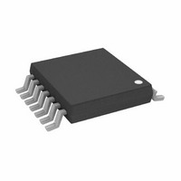
AD5292BRUZ-20 Analog Devices Inc, AD5292BRUZ-20 Datasheet - Page 28

AD5292BRUZ-20
Manufacturer Part Number
AD5292BRUZ-20
Description
IC POT DIG 1024P SPI 20K 14TSSOP
Manufacturer
Analog Devices Inc
Datasheet
1.AD5291BRUZ-20.pdf
(32 pages)
Specifications of AD5292BRUZ-20
Memory Type
Non-Volatile
Temperature Coefficient
35 ppm/°C Typical
Design Resources
30 V Low Cost DAC Using AD5292 Digital Potentiometer (CN0111) Variable Gain Noninverting Amplifier Using AD5292 and OP184 (CN0112) Variable Gain Inverting Amplifier Using AD5292 and OP184 (CN0113) Low Cost, High Voltage, Programmable Gain Instrumentation Amplifier Using AD5292 and AD8221 (CN0114) Programmable High Voltage Source with Boosted Output Current Using AD5292, OP184, and MOSFETs (CN0115) Programmable Bidirectional Current Source Using AD5292 and ADA4091-4 (CN0117) Logarithmic Audio Volume Control with Glitch Reduction Using AD5292 (CN0120)
Taps
1024
Resistance (ohms)
20K
Number Of Circuits
1
Interface
SPI Serial
Voltage - Supply
9 V ~ 33 V, ±9 V ~ 16.5 V
Operating Temperature
-40°C ~ 105°C
Mounting Type
Surface Mount
Package / Case
14-TSSOP
Resistance In Ohms
20K
End To End Resistance
20kohm
Resistance Tolerance
± 1%
No. Of Steps
1024
Control Interface
Serial, SPI
No. Of Pots
Single
Supply Voltage Range
± 9V To ± 16.5V
Rohs Compliant
Yes
Lead Free Status / RoHS Status
Lead free / RoHS Compliant
Other names
AD5292BRUZ-20-U1
AD5292BRUZ-20-U1
AD5292BRUZ-20-U1
Available stocks
Company
Part Number
Manufacturer
Quantity
Price
Company:
Part Number:
AD5292BRUZ-20
Manufacturer:
Micrel
Quantity:
100
Part Number:
AD5292BRUZ-20
Manufacturer:
ADI/亚德诺
Quantity:
20 000
AD5291/AD5292
APPLICATIONS INFORMATION
HIGH VOLTAGE DAC
The AD5292 can be configured as a high voltage DAC, with
output voltage as high as 33 V. The circuit is shown in Figure 70.
The output is
where D is the decimal code from 0 to 1023.
PROGRAMMABLE VOLTAGE SOURCE WITH
BOOSTED OUTPUT
For applications that require high current adjustments such as a
laser diode or tunable laser, a boosted voltage source can be
considered; see Figure 71.
In this circuit, the inverting input of the op amp forces V
be equal to the wiper voltage set by the digital potentiometer.
The load current is then delivered by the supply via the N-channel
FET (U3). The N-Channel FET power handling must be adequate
to dissipate (V
maximum of 100 mA with a 33 V supply.
ADR512
R
V
BIAS
OUT
V
DD
AD5292
(
D
D1
Figure 71. Programmable Boosted Voltage Source
U1
)
R
=
1
IN
V
1024
IN
B
− V
A
D
AD8512
V–
Figure 70. High Voltage DAC
OUT
×
W
V+
V
R
⎡
⎢
⎢
⎣
1
DD
OP184
2
) × I
2 .
U1A
V
L
U2
×
power. This circuit can source a
U3 2N7002
⎛
⎜
⎜
⎝
1
+
U2
AD5292
R
R
B
2
1
⎞
⎟
⎟
⎠
20kΩ
⎤
⎥
⎥
⎦
SIGNAL
LD
C
C
U1B
AD8512
R
V
BIAS
OUT
I
L
OUT
V
Rev. D | Page 28 of 32
to
OUT
(7)
HIGH ACCURACY DAC
It is possible to configure the AD5292 as a high accuracy DAC
by optimizing the resolution of the device over a specific
reduced voltage range. This is achieved by placing external
resistors on either side of the RDAC, as shown in Figure 72.
The improved ±1% R-Tolerance specification greatly reduces
error associated with matching to discrete resistors.
VARIABLE GAIN INSTRUMENTATION AMPLIFIER
The
the ADG1207, as shown in Figure 73, make an excellent
instrumentation amplifier for use in data acquisition systems.
The data acquisition system’s low distortion and low noise
enable it to condition signals in front of a variety of ADCs.
The gain can be calculated by using Equation 9.
AD8221
V
G
OUT
+V
+V
–V
–V
(
D
IN1
IN4
IN1
IN4
)
(
=
D
1
)
+
in conjunction with the AD5291 and AD5292 and
=
U1
AD5292
ADG1207
(
R
D
Figure 73. Data Acquisition System
1
Figure 72. Optimizing Resolution
20kΩ
1024
R
49
+
3
R
R
R
4 .
+
1
2
3
B
(
V
(
DD
kΩ
)
(
1024
D
±1%
×
1024
R
−
D
AB
)
×
AD5292
1024
R
)
AB
OP1177
×
V+
)
U2
V–
R
×
V
AB
V
DD
DD
+
R
AD8221
3
V
V
DD
SS
V
OUT
V
OUT
(8)
(9)


