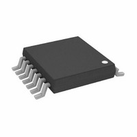
AD5292BRUZ-20 Analog Devices Inc, AD5292BRUZ-20 Datasheet - Page 27

AD5292BRUZ-20
Manufacturer Part Number
AD5292BRUZ-20
Description
IC POT DIG 1024P SPI 20K 14TSSOP
Manufacturer
Analog Devices Inc
Datasheet
1.AD5291BRUZ-20.pdf
(32 pages)
Specifications of AD5292BRUZ-20
Memory Type
Non-Volatile
Temperature Coefficient
35 ppm/°C Typical
Design Resources
30 V Low Cost DAC Using AD5292 Digital Potentiometer (CN0111) Variable Gain Noninverting Amplifier Using AD5292 and OP184 (CN0112) Variable Gain Inverting Amplifier Using AD5292 and OP184 (CN0113) Low Cost, High Voltage, Programmable Gain Instrumentation Amplifier Using AD5292 and AD8221 (CN0114) Programmable High Voltage Source with Boosted Output Current Using AD5292, OP184, and MOSFETs (CN0115) Programmable Bidirectional Current Source Using AD5292 and ADA4091-4 (CN0117) Logarithmic Audio Volume Control with Glitch Reduction Using AD5292 (CN0120)
Taps
1024
Resistance (ohms)
20K
Number Of Circuits
1
Interface
SPI Serial
Voltage - Supply
9 V ~ 33 V, ±9 V ~ 16.5 V
Operating Temperature
-40°C ~ 105°C
Mounting Type
Surface Mount
Package / Case
14-TSSOP
Resistance In Ohms
20K
End To End Resistance
20kohm
Resistance Tolerance
± 1%
No. Of Steps
1024
Control Interface
Serial, SPI
No. Of Pots
Single
Supply Voltage Range
± 9V To ± 16.5V
Rohs Compliant
Yes
Lead Free Status / RoHS Status
Lead free / RoHS Compliant
Other names
AD5292BRUZ-20-U1
AD5292BRUZ-20-U1
AD5292BRUZ-20-U1
Available stocks
Company
Part Number
Manufacturer
Quantity
Price
Company:
Part Number:
AD5292BRUZ-20
Manufacturer:
Micrel
Quantity:
100
Part Number:
AD5292BRUZ-20
Manufacturer:
ADI/亚德诺
Quantity:
20 000
Operation of the digital potentiometer in the voltage divider
mode results in a more accurate operation over temperature.
Unlike the rheostat mode, the output voltage is dependent
mainly on the ratio of the internal resistors, R
not the absolute values. Therefore, the temperature drift reduces
to 5 ppm/°C.
EXT_CAP CAPACITOR
A 1 μF capacitor to GND must be connected to the EXT_CAP
pin (see Figure 68) on power-up and throughout the operation
of the AD5291 and AD5292.
TERMINAL VOLTAGE OPERATING RANGE
The positive V
AD5291 and AD5292 define the boundary conditions for
proper 3-terminal digital potentiometer operation. Supply
signals present on Terminal A, Terminal B, and Terminal W
that exceed V
biased diodes (see Figure 69).
Figure 69. Maximum Terminal Voltages Set by V
DD
Figure 68. Hardware Setup for EXT_CAP Pin
DD
or V
and negative V
EXT_CAP
1µF
C1
SS
are clamped by the internal forward-
AD5291/
AD5292
MEMORY
SS
BLOCK
GND
OTP
power supplies of the
WA
DD
V
A
W
B
V
and R
DD
SS
and V
WB
SS
, and
Rev. D | Page 27 of 32
The ground pins of the AD5291 and AD5292 devices are
primarily used as a digital ground reference. To minimize the
digital ground bounce, the AD5291 and AD5292 ground
terminals should be joined remotely to the common ground.
The digital input control signals to the AD5291 and AD5292
must be referenced to the device ground pin (GND), and satisfy
the logic level defined in the Specifications section.
Power-Up Sequence
To ensure that the AD5291 and AD5292 power up correctly, a
1 μF capacitor must be connected to the EXT_CAP pin. Because
there are diodes to limit the voltage compliance at Terminal A,
Terminal B, and Terminal W (see Figure 69), it is important to
power V
Terminal B, and Terminal W. Otherwise, the diode is forward-
biased such that V
The ideal power-up sequence is GND, V
digital inputs, and then V
up V
they are powered after V
Regardless of the power-up sequence and the ramp rates of the
power supplies, after V
activates, restoring the 20-TP memory value to the RDAC register.
A
, V
DD
B
, V
and V
W
, and the digital inputs is not important as long as
SS
DD
first before applying any voltage to Terminal A,
and V
LOGIC
DD
A
, V
, V
SS
is powered, the power-on preset
are powered up unintentionally.
B
SS
, and V
, and V
W
LOGIC
AD5291/AD5292
. The order of powering
SS
, V
.
LOGIC
and V
DD
, the


