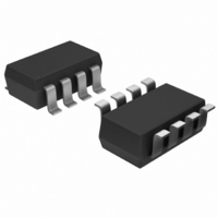
AD5171BRJZ5-R2 Analog Devices Inc, AD5171BRJZ5-R2 Datasheet - Page 12

AD5171BRJZ5-R2
Manufacturer Part Number
AD5171BRJZ5-R2
Description
IC DGTL POT OTP 5K I2C SOT23-8
Manufacturer
Analog Devices Inc
Datasheet
1.AD5171BRJZ10-R7.pdf
(24 pages)
Specifications of AD5171BRJZ5-R2
Memory Type
Non-Volatile
Temperature Coefficient
35 ppm/°C Typical
Taps
64
Resistance (ohms)
5K
Number Of Circuits
1
Interface
I²C, 2-Wire Serial
Voltage - Supply
2.7 V ~ 5.5 V
Operating Temperature
-40°C ~ 125°C
Mounting Type
Surface Mount
Package / Case
SOT-23-8
Resistance In Ohms
5K
End To End Resistance
5kohm
Resistance Tolerance
± 30%
No. Of Steps
64
Control Interface
Serial, I2C, 2-Wire
No. Of Pots
Single
Supply Voltage Range
2.7V To 5.5V
Rohs Compliant
Yes
Lead Free Status / RoHS Status
Lead free / RoHS Compliant
For Use With
AD5171EVAL - BOARD EVAL FOR AD5171
Lead Free Status / RoHS Status
Lead free / RoHS Compliant, Lead free / RoHS Compliant
Other names
AD5171BRJZ5-R2TR
Available stocks
Company
Part Number
Manufacturer
Quantity
Price
Company:
Part Number:
AD5171BRJZ5-R2
Manufacturer:
Microchip
Quantity:
446
AD5171
THEORY OF OPERATION
The AD5171 allows unlimited 6-bit adjustments, except for the
one-time programmable, set-and-forget resistance setting. OTP
technology is a proven, cost-effective alternative over EEMEM
in one-time memory programming applications. The AD5171
employs fuse link technology to achieve the memory retention
of the resistance setting function. It has six data fuses that control
the address decoder for programming the RDAC, one user
mode test fuse for checking setup error, and one programming
lock fuse for disabling any further programming once the data
fuses are blown.
ONE-TIME PROGRAMMING (OTP)
Prior to OTP activation, the AD5171 presets to midscale during
initial power-on. After the wiper is set at the desired position,
the resistance can be permanently set by programming the T bit
high along with the proper coding (see Table 8 and Table 9) and
one-time V
family of digital potentiometers requires V
and 5.25 V to blow the fuses to achieve a given nonvolatile
setting. On the other hand, V
operation. As a result, a system supply that is lower than 4.75 V
requires external supply for OTP. In addition, the user is only
allowed one attempt in blowing the fuses. If the user fails to
blow the fuses at the first attempt, the fuse structures may change
so that they may never be blown regardless of the energy applied
at subsequent events. For details, see the Power Supply
Considerations section.
The device control circuit has two validation bits, E1 and E0,
that can be read back to check the programming status (see
Table 5). Users should always read back the validation bits to
ensure that the fuses are properly blown. After the fuses are
blown, all fuse latches are enabled upon subsequent power-on;
therefore, the output corresponds to the stored setting.
DD_OTP
. The fuse link technology of the AD517x
SCL
SDA
DD
can be 2.7 V to 5.5 V during
CONTROL BLOCK
DD_OTP
PROGRAM/TEST
I
2
C INTERFACE
ONE-TIME
COMPARATOR
between 4.75 V
Figure 25. Detailed Functional Block Diagram
Rev. D | Page 12 of 24
FUSES
DAC
REG.
EN
Table 5. Validation Status
E1
0
0
1
1
This section discusses the fuse operation in detail. When the
OTP T bit is set, the internal clock is enabled. The program then
attempts to blow a test fuse. The operation stops if the test fuse
is not properly blown. The validation bits, E1 and E0, show 01.
This status is intended for factory setup checking purposes
only; users should not see this status. If the test fuse is properly
blown, the data fuses can be programmed. The six data fuses
are programmed in six clock cycles. The output of the fuses is
compared with the code stored in the RDAC register. If they do
not match, E1 and E0 of 10 are issued as fatal errors and the
operation stops. Users should never try blowing the fuses more
than once because the fuse structure may have changed prohibiting
further programming. As a result, the unit must be discarded.
This error status can also occur if the OTP supply voltage goes
above or drops below the V
current is limited, or both the voltage and current ramp times
are slow. If the output and stored code match, the programming
lock fuse is blown so that no further programming is possible.
In the meantime, E1 and E0 issue 11, indicating the lock fuse is
properly blown. All the fuse latches are enabled at power-on;
therefore, from this point on, the output corresponds to the
stored setting. Figure 25 shows a detailed functional block
diagram.
MUX
E0
0
1
0
1
FUSE
REG.
Status
Ready for programming.
Test fuse not blown successfully. For factory setup
checking purpose only. Users should not see these
combinations.
Fatal error. Some fuses are not blown. Do not retry.
Discard the unit.
Successful. No further programming is possible.
DECODER
DD_OTP
requirement, the OTP supply
A
W
B


