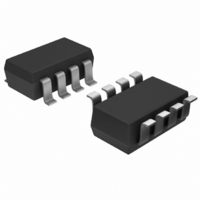
AD5171BRJZ5-R2 Analog Devices Inc, AD5171BRJZ5-R2 Datasheet - Page 17

AD5171BRJZ5-R2
Manufacturer Part Number
AD5171BRJZ5-R2
Description
IC DGTL POT OTP 5K I2C SOT23-8
Manufacturer
Analog Devices Inc
Datasheet
1.AD5171BRJZ10-R7.pdf
(24 pages)
Specifications of AD5171BRJZ5-R2
Memory Type
Non-Volatile
Temperature Coefficient
35 ppm/°C Typical
Taps
64
Resistance (ohms)
5K
Number Of Circuits
1
Interface
I²C, 2-Wire Serial
Voltage - Supply
2.7 V ~ 5.5 V
Operating Temperature
-40°C ~ 125°C
Mounting Type
Surface Mount
Package / Case
SOT-23-8
Resistance In Ohms
5K
End To End Resistance
5kohm
Resistance Tolerance
± 30%
No. Of Steps
64
Control Interface
Serial, I2C, 2-Wire
No. Of Pots
Single
Supply Voltage Range
2.7V To 5.5V
Rohs Compliant
Yes
Lead Free Status / RoHS Status
Lead free / RoHS Compliant
For Use With
AD5171EVAL - BOARD EVAL FOR AD5171
Lead Free Status / RoHS Status
Lead free / RoHS Compliant, Lead free / RoHS Compliant
Other names
AD5171BRJZ5-R2TR
Available stocks
Company
Part Number
Manufacturer
Quantity
Price
Company:
Part Number:
AD5171BRJZ5-R2
Manufacturer:
Microchip
Quantity:
446
Table 10. SDA Bits Definitions and Descriptions
Bit
S
P
A
AD0
X
T
D5, D4, D3, D2, D1, D0
E1, E0
I
Write Bit Patterns
Read Bit Pattern
I
For users who prefer to use external controllers, the AD5171
can be controlled via an I
connected to this bus as a slave device. The following section
describes how the 2-wire I
Figure 35, Figure 36, and Figure 37).
The master initiates data transfer by establishing a start condition,
which is when SDA goes from high to low while SCL is high
(see Figure 35 and Figure 36). The following byte is the slave
address byte, which consists of the 6 MSBs as a slave address
defined as 010110. The next bit is AD0, which is an I
address bit. Depending on the states of their AD0 bits, two
2
2
C CONTROLLER PROGRAMMING
C-COMPATIBLE 2-WIRE SERIAL BUS
START BY
START BY
MASTER
MASTER
SCL
SDA
SCL
SDA
1
0
1
0
1
1
START BY
SLAVE ADDRESS BYTE
SLAVE ADDRESS BYTE
MASTER
2
C-compatible serial bus; the part is
2
0
0
C serial bus protocol operates (see
Description
Start Condition.
Stop Condition.
Acknowledge.
I
Don’t Care.
OTP Programming Bit. Logic 1 programs the wiper position permanently.
Data Bits.
OTP Validation Bits:
0, 0 = Ready to Program.
0, 1 = Test Fuse Not Blown Successfully. For factory setup checking purpose only. Users should not see these
combinations.
1, 0 = Fatal Error. Do not retry. Discard the unit.
1, 1 = Programmed Successfully. No further adjustments are possible.
2
SCL
SDA
C Device Address Bit. Allows a maximum of two AD5171s to be addressed.
FRAME 1
FRAME 1
1
1
1
1
1
0
0
0 AD0 R/W
1
AD0 R/W
SLAVE ADDRESS BYTE
0
FRAME 1
ACK. BY
ACK. BY
AD5171
AD5171
1
9
Figure 36. Activating One-Time Programming
9
Figure 37. Reading Data from RDAC Register
1
Figure 35. Writing to the RDAC Register
2
C device
1
0
1
1
0 AD0
X
X
Rev. D | Page 17 of 24
X
X
INSTRUCTION BYTE
INSTRUCTION BYTE
R/W
ACK. BY
X
AD5171
X
FRAME 2
FRAME 2
9
X
X
E1
1
X
X
AD5171s can be addressed on the same bus (see Figure 38). The
last LSB is the R/ W bit, which determines whether data is read
from, or written to, the slave device.
The slave address corresponding to the transmitted address bit
responds by pulling the SDA line low during the 9
(this is termed the acknowledge bit). At this stage, all other
devices on the bus remain idle while the selected device waits
for data to be written to, or read from, its serial register.
The write operation contains one instruction byte more than
the read operation. The instruction byte in the write mode
follows the slave address byte. The MSB of the instruction byte
labeled T is the one-time programming bit. After acknowledging
E0
X
X
D5
RDAC REGISTER
X
X
D4
ACK. BY
ACK. BY
AD5171
AD5171
FRAME 2
9
9
D3
1
X
1
X
D2
X
X
D1
D5
D5
D0
NO ACK. BY
D4
D4
DATA BYTE
DATA BYTE
MASTER
FRAME 1
FRAME 1
9
D3
D3
STOP BY
MASTER
D2
D2
D1
D1
D0
D0
ACK. BY
ACK. BY
AD5171
AD5171
9
9
STOP BY
MASTER
STOP BY
MASTER
th
clock pulse
AD5171


