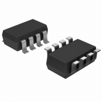
AD5171BRJZ5-R2 Analog Devices Inc, AD5171BRJZ5-R2 Datasheet - Page 20

AD5171BRJZ5-R2
Manufacturer Part Number
AD5171BRJZ5-R2
Description
IC DGTL POT OTP 5K I2C SOT23-8
Manufacturer
Analog Devices Inc
Datasheet
1.AD5171BRJZ10-R7.pdf
(24 pages)
Specifications of AD5171BRJZ5-R2
Memory Type
Non-Volatile
Temperature Coefficient
35 ppm/°C Typical
Taps
64
Resistance (ohms)
5K
Number Of Circuits
1
Interface
I²C, 2-Wire Serial
Voltage - Supply
2.7 V ~ 5.5 V
Operating Temperature
-40°C ~ 125°C
Mounting Type
Surface Mount
Package / Case
SOT-23-8
Resistance In Ohms
5K
End To End Resistance
5kohm
Resistance Tolerance
± 30%
No. Of Steps
64
Control Interface
Serial, I2C, 2-Wire
No. Of Pots
Single
Supply Voltage Range
2.7V To 5.5V
Rohs Compliant
Yes
Lead Free Status / RoHS Status
Lead free / RoHS Compliant
For Use With
AD5171EVAL - BOARD EVAL FOR AD5171
Lead Free Status / RoHS Status
Lead free / RoHS Compliant, Lead free / RoHS Compliant
Other names
AD5171BRJZ5-R2TR
Available stocks
Company
Part Number
Manufacturer
Quantity
Price
Company:
Part Number:
AD5171BRJZ5-R2
Manufacturer:
Microchip
Quantity:
446
AD5171
For log taper adjustment, such as volume control, Figure 44
shows another way of resistance scaling. In this circuit, the
smaller the R2 with respect to R
pseudo log taper characteristic. The wiper voltage is simply
RESOLUTION ENHANCEMENT
The resolution can be doubled in the potentiometer mode of
operation by using three digital potentiometers. Borrowed from
the Analog Devices patented RDAC segmentation technique,
users can configure three AD5171s to double the resolution (see
Figure 45). First, U3 must be parallel with a discrete resistor, R
which is chosen to be equal to a step resistance (R
Adjusting U1 and U2 together forms the coarse 6-bit adjustment,
and adjusting U3 alone forms the finer 6-bit adjustment. As a
result, the effective resolution becomes 12-bit.
V
Figure 44. Resistor Scaling with Log Adjustment Characteristics
W
(
D
)
=
R
WA
(
Figure 45. Doubling the Resolution
R
ADJUSTMENT
WB
+
COARSE
U1
U2
R
||
WB
A1
A2
B2
B1
R
R1
V
2
A
B
||
I
W1
W2
)
R
R
2
P
W
R2
×
ADJUSTMENT
AB
V
, the more it behaves like the
U3
I
FINE
V
O
A3
B3
W3
P
= R
AB
/64).
Rev. D | Page 20 of 24
(6)
P
,
RDAC CIRCUIT SIMULATION MODEL
The internal parasitic capacitances and the external capacitive
loads dominate the ac characteristics of the digital potentiometers.
Configured as a potentiometer divider, the –3 dB bandwidth of
the AD5171 (5 kΩ resistor) measures 1.5 MHz at half scale.
Figure 14 to Figure 17 provide the large signal BODE plot
characteristics of the four available resistor versions: 5 kΩ,
10 kΩ, 50 kΩ, and 100 kΩ. A parasitic simulation model is
shown in Figure 46. Listing 1 provides a macro model net list
for the 10 kΩ device.
Listing 1. Macro Model Net List for RDAC
.PARAM D=64, RDAC=10E3
*
.SUBCKT DPOT (A,W,B)
*
CA
RWA
CW
RWB
CB
*
.ENDS DPOT
A
A
W
W
B
Figure 46. Circuit Simulation Model for RDAC = 10 kΩ
0
W
0
B
0
A
C
25pF
A
W
RDAC
10kΩ
25E-12
{(1-D/64)*RDAC+60}
55E-12
{D/64*RDAC+60}
25E-12
55pF
C
W
C
25pF
B
B


