PIC18F65K90-I/MR Microchip Technology, PIC18F65K90-I/MR Datasheet - Page 22
PIC18F65K90-I/MR
Manufacturer Part Number
PIC18F65K90-I/MR
Description
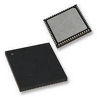
32kB Flash, 2kB RAM, 1kB EE, NanoWatt XLP, LCD 64 QFN 9x9x0.9mm TUBE
Manufacturer
Microchip Technology
Series
PIC® XLP™ 18Fr
Datasheet
1.PIC18F65K90-IMR.pdf
(570 pages)
Specifications of PIC18F65K90-I/MR
Processor Series
PIC18F
Core
PIC
Data Bus Width
8 bit
Program Memory Type
Flash
Program Memory Size
32 KB
Data Ram Size
2 KB
Interface Type
I2C, SPI
Maximum Clock Frequency
64 MHz
Number Of Timers
8
Operating Supply Voltage
1.8 V to 5.5 V
Maximum Operating Temperature
+ 125 C
3rd Party Development Tools
52715-96, 52716-328, 52717-734, 52712-325, EWPIC18
Minimum Operating Temperature
- 40 C
On-chip Adc
12 bit, 16 Channel
Core Processor
PIC
Core Size
8-Bit
Speed
64MHz
Connectivity
I²C, LIN, SPI, UART/USART
Peripherals
Brown-out Detect/Reset, LCD, POR, PWM, WDT
Number Of I /o
53
Eeprom Size
1K x 8
Ram Size
2K x 8
Voltage - Supply (vcc/vdd)
1.8 V ~ 5.5 V
Data Converters
A/D 16x12b
Oscillator Type
Internal
Operating Temperature
-40°C ~ 85°C
Package / Case
64-VFQFN Exposed Pad
Lead Free Status / Rohs Status
Details


PIC18F87K90 FAMILY
TABLE 1-3:
TABLE 1-4:
DS39957D-page 22
V
V
AV
AV
ENVREG
V
Legend: TTL
Note 1:
MCLR/RG5
RG5
OSC1/CLKI/RA7
OSC2/CLKO/RA6
Legend: TTL = TTL compatible input
Note 1:
SS
DD
DDCORE
SS
DD
V
V
OSC1
CLKI
RA7
OSC2
CLKO
RA6
DDCORE
CAP
2:
3:
2:
3:
4:
Pin Name
Pin Name
/V
ST
I
P
I
Default assignment for ECCP2 when the CCP2MX Configuration bit is set.
Alternate assignment for ECCP2 when the CCP2MX Configuration bit is cleared.
Not available on PIC18F65K90 and PIC18F85K90 devices.
ST
I
P
I
Default assignment for ECCP2 when the CCP2MX Configuration bit is set.
Alternate assignment for ECCP2 when the CCP2MX Configuration bit is cleared.
Not available on PIC18F65K90 and PIC18F85K90 devices.
The CCP6, CCP7, CCP8 and CCP9 pin placement depends on the ECCPMX Configuration bit setting.
CAP
2
2
C™ = I
C™ = I
= Schmitt Trigger input with CMOS levels
= Input
= Power
PIC18F6XK90 PINOUT I/O DESCRIPTIONS (CONTINUED)
PIC18F8XK90 PINOUT I/O DESCRIPTIONS
= TTL compatible input
= Schmitt Trigger input with CMOS levels
= Input
= Power
2
C/SMBus
2
C/SMBus
Pin Number
Pin Number
9, 25, 41, 56
QFN/TQFP
26, 38, 57
TQFP
20
19
18
10
49
50
9
Type
Type
Pin
Pin
I/O
I/O
O
O
P
P
P
P
P
I
I
I
I
I
Buffer
CMOS
CMOS
Buffer
Type
Type
TTL
TTL
ST
ST
ST
—
—
—
—
—
—
—
Master Clear (input) or programming voltage (input).
Oscillator crystal or external clock input.
Oscillator crystal or clock output.
Ground reference for logic and I/O pins.
Positive supply for logic and I/O pins.
Ground reference for analog modules.
Positive supply for analog modules.
Enable for on-chip voltage regulator.
Core logic power or external filter capacitor connection.
Oscillator crystal input.
External clock source input. Always associated
with pin function, OSC1. (See related OSC1/CLKI,
OSC2/CLKO pins.)
General purpose I/O pin.
Oscillator crystal output. Connects to crystal or
resonator in Crystal Oscillator mode.
In certain oscillator modes, OSC2 pin outputs CLKO,
which has 1/4 the frequency of OSC1 and denotes the
instruction cycle rate.
General purpose I/O pin.
This pin is an active-low Reset to the device.
General purpose, input only pin.
External filter capacitor connection (regulator
enabled/disabled).
CMOS = CMOS compatible input or output
Analog = Analog input
O
OD
CMOS = CMOS compatible input or output
Analog = Analog input
O
OD
= Output
= Open-Drain (no P diode to V
= Output
= Open-Drain (no P diode to V
Description
Description
2009-2011 Microchip Technology Inc.
DD
DD
)
)
Related parts for PIC18F65K90-I/MR
Image
Part Number
Description
Manufacturer
Datasheet
Request
R

Part Number:
Description:
Manufacturer:
Microchip Technology Inc.
Datasheet:
Part Number:
Description:
Manufacturer:
Microchip Technology Inc.
Datasheet:
Part Number:
Description:
Manufacturer:
Microchip Technology Inc.
Datasheet:
Part Number:
Description:
Manufacturer:
Microchip Technology Inc.
Datasheet:
Part Number:
Description:
Manufacturer:
Microchip Technology Inc.
Datasheet:
Part Number:
Description:
Manufacturer:
Microchip Technology Inc.
Datasheet:
Part Number:
Description:
Manufacturer:
Microchip Technology Inc.
Datasheet:
Part Number:
Description:
Manufacturer:
Microchip Technology Inc.
Datasheet: