PIC18F65K90-I/MR Microchip Technology, PIC18F65K90-I/MR Datasheet - Page 254
PIC18F65K90-I/MR
Manufacturer Part Number
PIC18F65K90-I/MR
Description
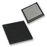
32kB Flash, 2kB RAM, 1kB EE, NanoWatt XLP, LCD 64 QFN 9x9x0.9mm TUBE
Manufacturer
Microchip Technology
Series
PIC® XLP™ 18Fr
Datasheet
1.PIC18F65K90-IMR.pdf
(570 pages)
Specifications of PIC18F65K90-I/MR
Processor Series
PIC18F
Core
PIC
Data Bus Width
8 bit
Program Memory Type
Flash
Program Memory Size
32 KB
Data Ram Size
2 KB
Interface Type
I2C, SPI
Maximum Clock Frequency
64 MHz
Number Of Timers
8
Operating Supply Voltage
1.8 V to 5.5 V
Maximum Operating Temperature
+ 125 C
3rd Party Development Tools
52715-96, 52716-328, 52717-734, 52712-325, EWPIC18
Minimum Operating Temperature
- 40 C
On-chip Adc
12 bit, 16 Channel
Core Processor
PIC
Core Size
8-Bit
Speed
64MHz
Connectivity
I²C, LIN, SPI, UART/USART
Peripherals
Brown-out Detect/Reset, LCD, POR, PWM, WDT
Number Of I /o
53
Eeprom Size
1K x 8
Ram Size
2K x 8
Voltage - Supply (vcc/vdd)
1.8 V ~ 5.5 V
Data Converters
A/D 16x12b
Oscillator Type
Internal
Operating Temperature
-40°C ~ 85°C
Package / Case
64-VFQFN Exposed Pad
Lead Free Status / Rohs Status
Details


features. They are:
PIC18F87K90 FAMILY
In addition to the expanded range of modes available
through the CCPxCON and ECCPxAS registers, the
ECCP modules have two additional registers associated
with Enhanced PWM operation and auto-shutdown
• ECCPxDEL – Enhanced PWM Control
• PSTRxCON – Pulse Steering Control
19.1
The Enhanced CCP module may have up to four PWM
outputs, depending on the selected operating mode.
The CCPxCON register is modified to allow control
over four PWM outputs: ECCPx/PxA, PxB, PxC and
PxD. Applications can use one, two or four of these
outputs.
The outputs that are active depend on the selected
ECCP operating mode. The pin assignments are
summarized in
To configure the I/O pins as PWM outputs, the proper
PWM mode must be selected by setting the PxM<1:0>
and CCPxM<3:0> bits. The appropriate TRIS direction
bits for the PORT pins must also be set as outputs.
19.1.1
The ECCP modules use Timers, 1, 2, 3, 4, 6, 8, 10 or 12,
depending on the mode selected. These timers are
available to CCP modules in Capture, Compare or PWM
modes, as shown in
TABLE 19-1:
DS39957D-page 254
Capture
Compare
PWM
ECCP Mode
ECCP Outputs and Configuration
ECCP MODULE AND TIMER
RESOURCES
Table
ECCP MODE – TIMER
RESOURCE
Timer2, Timer4, Timer6, Timer8,
Table
19-3.
Timer10 or Timer12
Timer1 or Timer3
Timer1 or Timer3
19-1.
Timer Resource
The assignment of a particular timer to a module is
determined by the timer to ECCP enable bits in the
CCPTMRSx register
between the two modules are depicted in
Capture operations are designed to be used when the
timer is configured for Synchronous Counter mode.
Capture operations may not work as expected if the
associated timer is configured for Asynchronous Counter
mode.
19.1.2
The pin assignment for ECCPx (capture input,
compare and PWM output) can change, based on
device configuration. The ECCPMX (CONFIG3H<1>)
Configuration bit determines which pins, ECCP1 and
ECCP3, are multiplexed to.
• Default/ECCPMX = 1:
• ECCPMX = 0:
The pin assignment for ECCP2 (capture input,
compare and PWM output) can change, based on
device configuration.
The CCP2MX Configuration bit (CONFIG3H<0>)
determines which pin, ECCP2, is multiplexed to.
• If CCP2MX = 1 (default) – ECCP2 is multiplexed
• If CCP2MX = 0 – ECCP2 is multiplexed to:
- ECCP1 (P1B/P1C) is multiplexed onto RE6
- ECCP3 (P3B/P3C) is multiplexed onto RE4
- ECCP1 (P1B/P1C) is multiplexed onto RH7
- ECCP3 (P3B/P3C) is multiplexed onto RH5
to RC1
- RE7 is the ECCP2 pin with CCP2MX = 0
and RE5
and RE3
and RH6
and RH4.
ECCP PIN ASSIGNMENT
2009-2011 Microchip Technology Inc.
(Register
19-2). The interactions
Figure
19-1.
Related parts for PIC18F65K90-I/MR
Image
Part Number
Description
Manufacturer
Datasheet
Request
R

Part Number:
Description:
Manufacturer:
Microchip Technology Inc.
Datasheet:
Part Number:
Description:
Manufacturer:
Microchip Technology Inc.
Datasheet:
Part Number:
Description:
Manufacturer:
Microchip Technology Inc.
Datasheet:
Part Number:
Description:
Manufacturer:
Microchip Technology Inc.
Datasheet:
Part Number:
Description:
Manufacturer:
Microchip Technology Inc.
Datasheet:
Part Number:
Description:
Manufacturer:
Microchip Technology Inc.
Datasheet:
Part Number:
Description:
Manufacturer:
Microchip Technology Inc.
Datasheet:
Part Number:
Description:
Manufacturer:
Microchip Technology Inc.
Datasheet: