PIC18F65K90-I/MR Microchip Technology, PIC18F65K90-I/MR Datasheet - Page 369
PIC18F65K90-I/MR
Manufacturer Part Number
PIC18F65K90-I/MR
Description
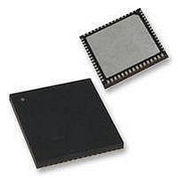
32kB Flash, 2kB RAM, 1kB EE, NanoWatt XLP, LCD 64 QFN 9x9x0.9mm TUBE
Manufacturer
Microchip Technology
Series
PIC® XLP™ 18Fr
Datasheet
1.PIC18F65K90-IMR.pdf
(570 pages)
Specifications of PIC18F65K90-I/MR
Processor Series
PIC18F
Core
PIC
Data Bus Width
8 bit
Program Memory Type
Flash
Program Memory Size
32 KB
Data Ram Size
2 KB
Interface Type
I2C, SPI
Maximum Clock Frequency
64 MHz
Number Of Timers
8
Operating Supply Voltage
1.8 V to 5.5 V
Maximum Operating Temperature
+ 125 C
3rd Party Development Tools
52715-96, 52716-328, 52717-734, 52712-325, EWPIC18
Minimum Operating Temperature
- 40 C
On-chip Adc
12 bit, 16 Channel
Core Processor
PIC
Core Size
8-Bit
Speed
64MHz
Connectivity
I²C, LIN, SPI, UART/USART
Peripherals
Brown-out Detect/Reset, LCD, POR, PWM, WDT
Number Of I /o
53
Eeprom Size
1K x 8
Ram Size
2K x 8
Voltage - Supply (vcc/vdd)
1.8 V ~ 5.5 V
Data Converters
A/D 16x12b
Oscillator Type
Internal
Operating Temperature
-40°C ~ 85°C
Package / Case
64-VFQFN Exposed Pad
Lead Free Status / Rohs Status
Details


22.3.2
Once Synchronous mode is selected, reception is
enabled by setting either the Single Receive Enable bit,
SREN (RCSTAx<5>), or the Continuous Receive
Enable bit, CREN (RCSTAx<4>). Data is sampled on
the RXx pin on the falling edge of the clock.
If enable bit, SREN, is set, only a single word is
received. If enable bit, CREN, is set, the reception is
continuous until CREN is cleared. If both bits are set,
then CREN takes precedence.
To set up a Synchronous Master Reception:
1.
2.
FIGURE 22-13:
2009-2011 Microchip Technology Inc.
RC6/TX1/CK1/
RC6/TX1/CK1/
Note:
RC7/RX1/DT1/
Initialize the SPBRGHx:SPBRGx registers for the
appropriate baud rate. Set or clear the BRG16
bit, as required, to achieve the desired baud rate.
Enable the synchronous master serial port by
setting bits, SYNC, SPEN and CSRC.
(TXCKP = 0)
(TXCKP = 1)
SEG27 Pin
SEG27 Pin
SEG28 Pin
bit, SREN
(Interrupt)
RC1IF bit
SREN bit
CREN bit
RCREG1
Write to
Timing diagram demonstrates Sync Master mode with bit, SREN = 1, and bit, BRGH = 0. This example is equally applicable to EUSART2
(RG1/TX2/CK2/AN19/C3OUT and RG2/RX2/DT2/AN18/C3INA).
Read
EUSART SYNCHRONOUS
MASTER RECEPTION
Q2
‘0’
Q3 Q4 Q1 Q2 Q3 Q4 Q1 Q2 Q3 Q4
SYNCHRONOUS RECEPTION (MASTER MODE, SREN)
bit 0
Q1 Q2 Q3 Q4 Q1 Q2 Q3 Q4 Q1 Q2 Q3 Q4 Q1 Q2 Q3 Q4 Q1 Q2 Q3 Q4 Q1 Q2 Q3 Q4 Q1 Q2 Q3 Q4
bit 1
bit 2
bit 3
PIC18F87K90 FAMILY
3.
4.
5.
6.
7.
8.
9.
10. If any error occurred, clear the error by clearing
11. If using interrupts, ensure that the GIE and PEIE bits
Ensure bits, CREN and SREN, are clear.
If interrupts are desired, set enable bit, RCxIE.
If 9-bit reception is desired, set bit, RX9.
If a single reception is required, set bit, SREN.
For continuous reception, set bit, CREN.
Interrupt flag bit, RCxIF, will be set when recep-
tion is complete and an interrupt will be generated
if the enable bit, RCxIE, was set.
Read the RCSTAx register to get the 9th bit (if
enabled) and determine if any error occurred
during reception.
Read the 8-bit received data by reading the
RCREGx register.
bit CREN.
in the INTCON register (INTCON<7:6>) are set.
bit 4
bit 5
bit 6
DS39957D-page 369
bit 7
Q1 Q2 Q3 Q4
‘0’
Related parts for PIC18F65K90-I/MR
Image
Part Number
Description
Manufacturer
Datasheet
Request
R

Part Number:
Description:
Manufacturer:
Microchip Technology Inc.
Datasheet:
Part Number:
Description:
Manufacturer:
Microchip Technology Inc.
Datasheet:
Part Number:
Description:
Manufacturer:
Microchip Technology Inc.
Datasheet:
Part Number:
Description:
Manufacturer:
Microchip Technology Inc.
Datasheet:
Part Number:
Description:
Manufacturer:
Microchip Technology Inc.
Datasheet:
Part Number:
Description:
Manufacturer:
Microchip Technology Inc.
Datasheet:
Part Number:
Description:
Manufacturer:
Microchip Technology Inc.
Datasheet:
Part Number:
Description:
Manufacturer:
Microchip Technology Inc.
Datasheet: