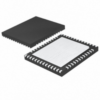
LTC2754BIUKG-16#PBF Linear Technology, LTC2754BIUKG-16#PBF Datasheet - Page 11

LTC2754BIUKG-16#PBF
Manufacturer Part Number
LTC2754BIUKG-16#PBF
Description
IC DAC 16BIT QUAD IOUT 52-QFN
Manufacturer
Linear Technology
Datasheet
1.LTC2754IUKG-12PBF.pdf
(28 pages)
Specifications of LTC2754BIUKG-16#PBF
Settling Time
2µs
Number Of Bits
16
Data Interface
Serial, SPI™
Number Of Converters
4
Voltage Supply Source
Single Supply
Operating Temperature
-40°C ~ 85°C
Mounting Type
Surface Mount
Package / Case
52-QFN
Lead Free Status / RoHS Status
Lead free / RoHS Compliant
Power Dissipation (max)
-
R
pin provides the translation of the output voltage range for
bipolar spans. Accepts up to ±15V; for normal operation
tie to the positive reference voltage at R
impedance looking into this pin is 20k to ground.
REFA (Pin 51): Inverted Reference Voltage for DAC A, with
internal connection to the reference inverting resistor. The
20k resistor is connected internally from REFA to R
For normal operation tie this pin to the output of reference
inverting amplifi er (see Typical Applications). Typically –5V;
BLOCK DIAGRAM
PIN FUNCTIONS
OFSA
(Pin 50): Bipolar Offset Network for DAC A. This
V
V
GE
GE
OSADJA
OSADJD
R
R
I
I
I
I
R
R
OUT2D
OUT1D
OUT1A
OUT2A
COMA
REFD
COMD
REFA
R
R
OFSD
ADJD
R
R
ADJA
OFSA
FBA
FBD
IND
INA
52
51
50
49
48
47
20
12
19
18
17
16
15
14
13
2
1
3
2.56M
2.56M
GND
4, 11, 37
10
SPAN SELECT
SPAN SELECT
16-BIT WITH
16-BIT WITH
V
DAC A
DAC D
DD
20k
20k
20k
20k
M-SPAN
32
POWER-ON
16
16
3
3
RESET
35
S2
DAC REG
DAC REG
DAC REG
DAC REG
SPAN REGISTERS
SPAN REGISTERS
DATA REGISTERS
DATA REGISTERS
INA
S1
34
(Pin 2). The
33
S0
CONTROL AND READBACK LOGIC
INPUT REG
INPUT REG
INPUT REG
INPUT REG
COMA
RFLAG
31
LTC2754-16
.
accepts up to ±15V. The impedance looking into this pin
is 10k to ground (R
R
Inverting Resistors. The 20k reference inverting resistors
are connected internally from R
R
normal operation tie R
reference inverting amplifi er (see Typical Applications).
Exposed Pad (Pin 53): Ground. The Exposed Pad must
be soldered to the PCB.
CLR
INPUT REG
INPUT REG
INPUT REG
INPUT REG
30
COMA
COMA
SPAN REGISTERS
SPAN REGISTERS
DATA REGISTERS
DATA REGISTERS
CS/LD
(Pin 52): Center Tap Point for Reference Amplifi er
to REFA, respectively (see Block Diagram). For
5
DAC REG
DAC REG
DAC REG
DAC REG
SDI
6
SCK
7
LDAC
16
16
3
3
36
INA
COMA
SRO
SPAN SELECT
SPAN SELECT
SPAN SELECT
and R
16-BIT WITH
16-BIT WITH
16-BIT WITH
8
DAC B
DAC B
DAC C
to the negative input of external
20k
20k
20k
20k
COMA
9
SROGND
2.56M
2.56M
INA
fl oating).
2754 BD
to R
39
40
41
42
43
44
45
38
46
21
29
22
23
24
25
26
27
28
LTC2754
R
GE
R
REFB
R
R
I
I
V
V
I
I
R
R
REFC
R
GE
R
OUT1B
OUT2B
OUT2C
OUT1C
OSADJB
OSADJC
COMA
INB
COMB
OFSB
FBB
FBC
OFSC
COMC
INC
ADJB
ADJC
and from
11
2754f


