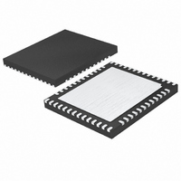
LTC2754BIUKG-16#PBF Linear Technology, LTC2754BIUKG-16#PBF Datasheet - Page 13

LTC2754BIUKG-16#PBF
Manufacturer Part Number
LTC2754BIUKG-16#PBF
Description
IC DAC 16BIT QUAD IOUT 52-QFN
Manufacturer
Linear Technology
Datasheet
1.LTC2754IUKG-12PBF.pdf
(28 pages)
Specifications of LTC2754BIUKG-16#PBF
Settling Time
2µs
Number Of Bits
16
Data Interface
Serial, SPI™
Number Of Converters
4
Voltage Supply Source
Single Supply
Operating Temperature
-40°C ~ 85°C
Mounting Type
Surface Mount
Package / Case
52-QFN
Lead Free Status / RoHS Status
Lead free / RoHS Compliant
Power Dissipation (max)
-
OPERATION
Input and DAC Registers
The LTC2754 has 5 internal registers for each DAC, a total
of 20 registers (see Block Diagram). Each DAC channel
has two sets of double-buffered registers—one set for the
code data, and one for the output range of the DAC—plus
one readback register. Double buffering provides the ca-
pability to simultaneously update the span (output range)
and code, which allows smooth voltage transitions when
changing output ranges. It also permits the simultaneous
updating of multiple DACs.
Each set of double-buffered registers comprises an Input
register and a DAC register.
Input register: The Write operation shifts data from the
SDI pin into a chosen Input register. The Input registers
are holding buffers; Write operations do not affect the
DAC outputs.
DAC register: The Update operation copies the contents
of an Input register to its associated DAC register. The
contents of a DAC register directly updates the associated
DAC output voltage or output range.
Note that updates always include both Data and Span
registers; but the values held in the DAC registers will
only change if the associated Input register values have
previously been changed via a Write operation.
Serial Interface
When the CS/LD pin is taken low, the data on the SDI
pin is loaded into the shift register on the rising edge of
the clock (SCK pin). The minimum (24-bit wide) loading
sequence required for the LTC2754 is a 4-bit command
word (C3 C2 C1 C0), followed by a 4-bit address word
(A3 A2 A1 A0) and 16 data (span or code) bits, MSB fi rst.
Figure 2 shows the SDI input word syntax to use when
writing code or span. If a 32-bit input sequence is used,
the fi rst eight bits must be zeros, followed by the same
sequence as for a 24-bit wide input. Figure 3 shows the
input and readback sequences for both 24-bit and 32-bit
operations.
When CS/LD is low, the SRO pin (Serial Readback Output)
is an active output.The readback data begins after the
command (C3-C0) and address (A3-A0) words have been
shifted into SDI. SRO outputs a logic low until the readback
data begins. For a 24-bit input sequence, the 16 readback
bits are shifted out on the falling edges of clocks 8-23,
suitable for shifting into a microprocessor on the rising
edges of clocks 9-24. For a 32-bit sequence, the bits are
shifted out on clocks 16-31; see Figure 3b.
When CS/LD is high, the SRO pin presents a high impedance
(three-state) output.
LDAC is an asynchronous update pin. When LDAC is
taken low, all DACs are updated with code and span data
(data in the Input buffers is copied into the DAC buffers).
CS/LD must be high during this operation; otherwise
LDAC is locked out and will have no effect. The use of
LDAC is functionally identical to the “Update All DACs”
serial input command.
The codes for the command word (C3-C0) are defi ned in
Table 1; Table 2 defi nes the codes for the address word
(A3-A0).
Readback
In addition to the Input and DAC registers, each DAC has
one Readback register associated with it. When a Read
command is issued to a DAC, the contents of one of its
four buffers (Input and DAC registers for each of Span
and Code) is copied into its Readback register and seri-
ally shifted out through the SRO pin. Figure 3 shows the
loading and readback sequences.
In the data fi eld (D15-D0) of any non-read instruction cycle,
SRO shifts out the contents of the buffer that was specifi ed
in the preceding command. This “rolling readback” default
mode of operation can dramatically reduce the number
of instruction cycles needed, since any command can be
verifi ed during succeeding commands with no additional
overhead. See Figure 4. Table 1 shows the storage location
(‘readback pointer’) of the data which will be output from
SRO during the next instruction.
For Read commands, the data is shifted out during the Read
instruction itself (on the 16 falling SCK edges immediately
after the last address bit is shifted in on SDI). When checking
the span of a DAC using SRO, the span bits are the last
four bits shifted out, corresponding to their sequence and
positions when writing a span. See Figure 3.
LTC2754
13
2754f


