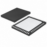
LTC2754BIUKG-16#PBF Linear Technology, LTC2754BIUKG-16#PBF Datasheet - Page 20

LTC2754BIUKG-16#PBF
Manufacturer Part Number
LTC2754BIUKG-16#PBF
Description
IC DAC 16BIT QUAD IOUT 52-QFN
Manufacturer
Linear Technology
Datasheet
1.LTC2754IUKG-12PBF.pdf
(28 pages)
Specifications of LTC2754BIUKG-16#PBF
Settling Time
2µs
Number Of Bits
16
Data Interface
Serial, SPI™
Number Of Converters
4
Voltage Supply Source
Single Supply
Operating Temperature
-40°C ~ 85°C
Mounting Type
Surface Mount
Package / Case
52-QFN
Lead Free Status / RoHS Status
Lead free / RoHS Compliant
Power Dissipation (max)
-
LTC2754
Op Amp Selection
Because of the extremely high accuracy of the 16-bit
LTC2754-16, careful thought should be given to op amp
selection in order to achieve the exceptional performance
of which the part is capable. Fortunately, the sensitivity of
INL and DNL to op amp offset has been greatly reduced
compared to previous generations of multiplying DACs.
Tables 4 and 5 contain equations for evaluating the effects
of op amp parameters on the LTC2754’s accuracy when
programmed in a unipolar or bipolar output range. These
are the changes the op amp can cause to the INL, DNL,
unipolar offset, unipolar gain error, bipolar zero and bipolar
gain error. Tables 4 and 5 can also be used to determine
the effects of op amp parameters on the LTC2754-12.
However, the results obtained from Tables 4 and 5 are
APPLICATIONS INFORMATION
Table 5. Easy-to-Use Equations Determine Op Amp Effects on DAC Accuracy in All Output Ranges (Circuit of Page 1). Subscript 1
Refers to Output Amp, Subscript 2 Refers to Reference Inverting Amp.
Table 6. Partial List of LTC Precision Amplifi ers Recommended for Use with the LTC2754 with Relevant Specifi cations
AMPLIFIER
LT1001
LT1097
LT1112 (Dual)
LT1124 (Dual)
LT1468
LT1469 (Dual)
20
A
A
V
V
VOL1
VOL2
I
OP AMP
OS1
I
OS2
B2
B1
(mV)
(nA)
(mV)
(mV)
(V/V)
(V/V)
I
B1
V
OS1
• 0.0003 •
A1 •
INL (LSB)
• 3.2 •
(
0
0
0
A
16.5k
V
125
μV
25
50
60
70
75
VOL1
OS
( )
( )
V
V
5V
REF
5V
REF
)
I
B1
V
0.35
0.25
nA
OS1
20
10
10
I
2
B
• 0.00008 •
DNL (LSB)
A2 •
• 0.82 •
(
0
0
0
A
1.5k
VOL1
V/mV
A
1000
1500
4000
5000
2000
( )
800
V
( )
VOL
V
5V
REF
5V
REF
)
A3 • V
VOLTAGE
nV/√Hz
I
NOISE
B1
OFFSET (LSB)
2.7
10
14
14
OS1
5
5
UNIPOLAR
• 0.13 •
• 13.2 •
0
0
0
0
AMPLIFIER SPECIFICATIONS
CURRENT
( )
V
pA/√Hz
NOISE
5V
0.008
0.008
REF
0.12
( )
0.3
0.6
0.6
V
5V
REF
in 16-bit LSBs. Divide these results by 16 to obtain the
correct LSB sizing.
Table 6 contains a partial list of LTC precision op amps
recommended for use with the LTC2754. The easy-to-use
design equations simplify the selection of op amps to meet
Table 4. Coeffi cients for the Equations in Table 5
OUTPUT RANGE
A4 • V
–2.5V to 7.5V
A3 • V
A4 • I
I
B1
SLEW
±2.5V
(
RATE
±10V
V/μs
0.25
0.16
BIPOLAR ZERO
(
10V
±5V
0.2
4.5
5V
ERROR (LSB)
22
22
OS1
OS2
B2
A4 •
• 0.13 •
• 0.13 •
• 19.8 •
• 13.1 •
(
0
A
66k
VOL2
( )
V
GAIN BANDWIDTH
5V
REF
( )
V
( )
( )
)
V
5V
V
REF
PRODUCT
5V
5V
REF
REF
1.1
2.2
1.9
A1
MHz
0.75
12.5
2
4
1
0.8
0.7
)
90
90
)
I
V
B1
V
OS1
I
UNIPOLAR GAIN
OS2
B2
ERROR (LSB)
• 0.0018 •
A5 •
• 0.26 •
• 13.2 •
A2
• 26.2 •
(
2
3
2
4
1
3
A
131k
VOL2
(
A
with LTC2755
131k
VOL1
( )
t
( )
)
V
( )
( )
SETTLING
V
V
V
5V
REF
0.83
5V
REF
5V
5V
120
120
115
0.5
1.4
0.7
A3
REF
REF
μs
19
1
1
2
2
)
V
V
I
B1
OS1
I
OS2
B2
BIPOLAR GAIN
ERROR (LSB)
0.5
• 0.0018 •
A4
A5 •
1
1
1
• 0.26 •
• 13.2 •
DISSIPATION
10.5/Op Amp
• 26.2 •
(
123/Op Amp
69/Op Amp
A
131k
VOL2
POWER
(
A
mW
117
131k
46
11
VOL1
( )
)
( )
( )
V
1.5
1.5
2.5
1.5
V
A5
( )
V
5V
1
1
5V
V
REF
REF
5V
REF
5V
2754f
REF
)


