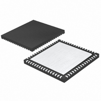
LTC2755BIUP-16#PBF Linear Technology, LTC2755BIUP-16#PBF Datasheet - Page 10

LTC2755BIUP-16#PBF
Manufacturer Part Number
LTC2755BIUP-16#PBF
Description
IC DAC 16BIT CUR OUT 64-QFN
Manufacturer
Linear Technology
Datasheet
1.LTC2755IUP-12PBF.pdf
(24 pages)
Specifications of LTC2755BIUP-16#PBF
Settling Time
2µs
Number Of Bits
16
Data Interface
Parallel
Number Of Converters
4
Voltage Supply Source
Single Supply
Operating Temperature
-40°C ~ 85°C
Mounting Type
Surface Mount
Package / Case
64-QFN
Lead Free Status / RoHS Status
Lead free / RoHS Compliant
Power Dissipation (max)
-
Available stocks
Company
Part Number
Manufacturer
Quantity
Price
PIN FUNCTIONS
LTC2755
R
is ±5V. The impedance looking into this pin is 1M to ground.
If not used, tie R
R
is ±5V. The impedance looking into this pin is 1M to ground.
If not used, tie R
I
ground when the DAC is operating and should reside at
0V. For normal operation tie to the negative input of the I/V
converter amplifi er for DAC C (see Typical Applications).
R
operation tie to the output of the I/V converter amplifi er
for DAC C (see Typical Applications). The DAC output
current from I
to the R
10k to ground.
R
pin provides the translation of the output voltage range for
bipolar spans. Accepts up to ±15V; for normal operation
tie to the positive reference voltage at R
impedance looking into this pin is 20k to ground.
REFC (Pin 30): Reference Input for DAC C, and connec-
tion for internal reference inverting resistor R4. The 20k
resistor R4 is connected internally from R
For normal operation tie this pin to the output of reference
inverting amplifi er A2 (see Typical Applications). Typically
–5V; accepts up to ±15V. The impedance looking into this
pin is 10k to ground (R
R
fier A2 Inverting Resistors. The 20k reference inverting
resistors R3 and R4 are connected internally from R
R
Diagram). For normal operation tie R
input of external reference inverting amplifier A2 (see
Typical Applications).
R
Amplifier A2. The 20k resistor R3 is connected internally
from R
external reference voltage V
Typically 5V; accepts up to ±15V.
MSPAN (Pin 33): Manual Span Control Pin. MSPAN is used
to confi gure the LTC2755 for operation in a single, fi xed
10
OUT1C
VOSD
VOSC
FBC
OFSC
COM2
COM2
IN2
(Pin 32): Input Resistor R3 for Reference Inverting
(Pin 28): DAC C Feedback Resistor. For normal
(Pin 25): DAC D Offset Adjust. Nominal input range
(Pin 26): DAC C Offset Adjust. Nominal input range
(Pin 27): DAC C Current Output. This pin is a virtual
(Pin 29): Bipolar Offset Network for DAC C. This
(Pin 31): Center Tap Point for the Reference Ampli-
IN2
and from R
FBC
to R
pin. The impedance looking into this pin is
OUT1C
COM2
VOSD
VOSC
COM2
. For normal operation tie R
fl ows through the feedback resistor
to ground.
to ground.
IN2
to REFC, respectively (see Block
REF2
and R
(see Typical Applications).
COM2
COM2
fl oating).
IN2
to the negative
COM2
(Pin 32). The
IN2
to REFC.
to the
IN2
to
output range. When confi gured for single-span operation,
the output range is set via hardware pin strapping. The
span I/O port’s input, and DAC, registers are transparent
and do not respond to write or update commands.
To confi gure the part for single-span use, tie MSPAN directly
to V
confi guration), the output ranges are set and verifi ed by
using write, update and read operations. See Manual Span
Confi guration in the Operation section. MSPAN must be
connected either directly to GND (SoftSpan confi guration)
or V
I
I
GND (Pin 35): Shield Ground, provides necessary shield-
ing for I
D0-D2 (Pins 36-38): LTC2755-12 Only. DAC Input/Output
Data Bits. These I/O pins set and read back the DAC code.
D0 is the LSB.
D0-D4 (Pins 36-40): LTC2755-14 Only. DAC Input/Output
Data Bits. These I/O pins set and read back the DAC code.
D0 is the LSB.
D0-D6 (Pins 36-42): LTC2755-16 Only. DAC Input/Output
Data Bits. These I/O pins set and read back the DAC code.
D0 is the LSB.
NC (Pins 39-44): LTC2755-12 Only. No Internal Connection.
NC (Pins 41-44): LTC2755-14 Only. No Internal Connection.
NC (Pins 43-44): LTC2755-16 Only. No Internal Connection.
GND (Pin 45): Shield Ground, provides necessary shield-
ing for I
I
I
S0 (Pin 47): Span I/O Bit 0. Pins S0, S1 and S2 are used
to program and to read back the output ranges of the
DACs.
D/S (Pin 48): Data/Span Select. This pin is used to select
the data I/O port or the span I/O port (D0 to D15 or S0 to
S2, respectively), along with their respective dedicated
registers, for write and read operations. Update opera-
tions ignore D/S, since all updates affect both data and
span registers. See Table 1. For single-span operation,
tie D/S to ground.
OUT2C
OUT2C
OUT2B
OUT2B
DD
DD
. If MSPAN is instead connected to GND (SoftSpan
, Pin 15 (single-span confi guration).
(Pin 34): DAC C Current Output Complement. Tie
to ground.
(Pin 46): DAC B Current Output Complement. Tie
to ground.
OUT2C
OUT2B
. Tie to ground.
. Tie to ground.
2755f


