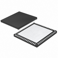
LTC2755BIUP-16#PBF Linear Technology, LTC2755BIUP-16#PBF Datasheet - Page 6

LTC2755BIUP-16#PBF
Manufacturer Part Number
LTC2755BIUP-16#PBF
Description
IC DAC 16BIT CUR OUT 64-QFN
Manufacturer
Linear Technology
Datasheet
1.LTC2755IUP-12PBF.pdf
(24 pages)
Specifications of LTC2755BIUP-16#PBF
Settling Time
2µs
Number Of Bits
16
Data Interface
Parallel
Number Of Converters
4
Voltage Supply Source
Single Supply
Operating Temperature
-40°C ~ 85°C
Mounting Type
Surface Mount
Package / Case
64-QFN
Lead Free Status / RoHS Status
Lead free / RoHS Compliant
Power Dissipation (max)
-
Available stocks
Company
Part Number
Manufacturer
Quantity
Price
LTC2755
TIMING CHARACTERISTICS
otherwise specifi cations are at T
SYMBOL
V
t
t
t
CLR Timing
t
Note 1: Stresses beyond those listed under Absolute Maximum Ratings
may cause permanent damage to the device. Exposure to any Absolute
Maximum Rating condition for extended periods may affect device
reliability and lifetime.
Note 2: Continuous operation above the specifi ed maximum operating
junction temperature may impair device reliability.
Note 3: Because of the proprietary SoftSpan switching architecture, the
measured resistance looking into each of the specifi ed pins is constant for
all output ranges if the I
Note 4: R1 measured from R
R
R
Note 5: Using LT1469 with C
of 1.7μs can be achieved by optimizing the time constant on an individual
basis. See Application Note 74, Component and Measurement Advances
Ensure 16-Bit DAC Settling Time.
LTC2755-16
TYPICAL PERFORMANCE CHARACTERISTICS
6
22
23
24
25
DD
COM1;
COM2
–0.2
–0.4
–0.6
–1.0
–0.8
= 2.7V to 3.3V
0.2
1.0
0.8
0.6
0.4
0.0
.
R3 measured from R
Integral Nonlinearity (INL)
0
V
V
±10V RANGE
DD
REF
= 5V
= 5V
PARAMETER
READ Falling Edge to UPD Rising Edge
I/O Bus Hi-Z to Read Rising Edge
Read Falling Edge to I/O Bus Active
CLR Pulse Width Low
16384
OUT1X
32768
CODE
FEEDBACK
IN2
IN1
and I
to R
to R
OUT2X
49152
COM2
COM1
A
= 15pF . A ±0.0015% settling time
= 25°C.
pins are held at ground.
; R4 measured from REFC to
; R2 measured from REFA to
2755 G01
65535
–0.2
–0.4
–0.6
–0.8
–1.0
0.2
1.0
0.8
0.6
0.4
0.0
The
0
Differential Nonlinearity (DNL)
V
V
±10V RANGE
DD
REF
CONDITIONS
(Note 11)
(Note 11)
(Note 11)
●
= 5V
= 5V
denotes specifi cations that apply over the full operating temperature range,
16384
32768
CODE
Note 6: Measured at the major carry transition, 0V to 5V range. Output
amplifi er: LT1469; C
Note 7. Full-scale transition; REF = 0V.
Note 8. Analog Crosstalk is defi ned as the AC voltage ratio V
expressed in dB. REFB is grounded, and DAC B is set to 0V-5V span and
zero-, mid- or full- scale code. V
between other DAC channels is similar or better.
Note 9. REF = 6V
amplifi er = LT1469.
Note 10. Calculation from V
(Boltzmann constant), R = resistance (Ω), T = temperature (°K), and B =
bandwidth (Hz). 0V to 5V Range; zero-, mid-, or full- scale.
Note 11. Guaranteed by design, not subject to test.
49152
2755 G02
T
A
RMS
65535
= 25°C, unless otherwise noted.
FB
at 1kHz. 0V to 5V range. DAC code = FS. Output
= 27pF .
n
–0.2
–0.4
–0.6
–1.0
–0.8
●
●
●
●
= √ ⎯ 4 ⎯ k ⎯ T ⎯ R ⎯ ⎯ ⎯ B , where k = 1.38E-23 J/°K
0.2
1.0
0.8
0.6
0.4
0.0
REFA
–40
INL vs Temperature
V
V
±10V RANGE
DD
REF
MIN
is a 3V
10
35
20
0
= 5V
–20
= 5V
RMS
TEMPERATURE (°C)
0
, 1kHz sine wave. Crosstalk
TYP
+INL
–INL
20
40
MAX
OUTB
60
/V
REFA
2755 G04
UNITS
80
2755f
,
ns
ns
ns
ns


