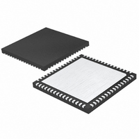
LTC2755BIUP-16#PBF Linear Technology, LTC2755BIUP-16#PBF Datasheet - Page 3

LTC2755BIUP-16#PBF
Manufacturer Part Number
LTC2755BIUP-16#PBF
Description
IC DAC 16BIT CUR OUT 64-QFN
Manufacturer
Linear Technology
Datasheet
1.LTC2755IUP-12PBF.pdf
(24 pages)
Specifications of LTC2755BIUP-16#PBF
Settling Time
2µs
Number Of Bits
16
Data Interface
Parallel
Number Of Converters
4
Voltage Supply Source
Single Supply
Operating Temperature
-40°C ~ 85°C
Mounting Type
Surface Mount
Package / Case
64-QFN
Lead Free Status / RoHS Status
Lead free / RoHS Compliant
Power Dissipation (max)
-
Available stocks
Company
Part Number
Manufacturer
Quantity
Price
ELECTRICAL CHARACTERISTICS
specifi cations which apply over the full operating temperature range, otherwise specifi cations are at T
SYMBOL PARAMETER
Static Performance
DNL
INL
GE
GE
BZE
BZS
PSR
I
C
V
otherwise specifi cations are at T
SYMBOL
Resistances (Note 3)
R1, R2, R3, R4
R
R
R
R
Dynamic Performance
THD
LKG
IOUT1
VOS
DD
REF
FB
OFS
TC
TC
= 5V, V
Resolution
Monotonicity
Differential
Nonlinearity
Integral
Nonlinearity
Gain Error
Gain Error Temp-
erature Coeffi cient
Bipolar Zero Error
Bipolar Zero Temp-
erature Coeffi cient
Power Supply
Rejection
I
Current
Output
Capacitance
OUT1
REF
Leakage
= 5V unless otherwise specifi ed. The
PARAMETER
Reference Inverting Resistors
DAC Input Resistance
Feedback Resistor
Bipolar Offset Resistor
Offset Adjust Resistor
Output Settling Time
Glitch Impulse
Digital-to-Analog Glitch Impulse
Reference Multiplying BW
Multiplying Feedthrough Error
Analog Crosstalk
Total Harmonic Distortion
Output Noise Voltage Density
CONDITIONS
All Output
Ranges
ΔGain/ΔTemp
All Bipolar
Ranges
V
V
T
T
Full-Scale
Zero Scale
A
DD
DD
MIN
= 25°C
= 5V, ±10%
= 3V, ±10%
A
to T
= 25°C.
MAX
●
●
●
●
●
●
●
●
●
MIN
12
12
LTC2755-12
●
CONDITIONS
(Note 4)
(Note 3)
(Note 3)
0V to 10V Range, 10V Step. To ±0.0015% FS
(Note 5)
(Note 6)
(Note 7)
0V to 5V Range, V
code = Full Scale, –3dB BW
0V to 5V Range, V
Sine Wave
(Note 8)
(Note 9) Multiplying
(Note 10) at I
±0.05
±0.5
±0.6
±0.2
±0.5
TYP
denotes specifi cations that apply over the full operating temperature range,
75
45
V
DD
±0.025
±0.06
MAX
±1
±1
±2
±1
±2
±5
= 5V, V
OUT1
MIN
REF
REF
14
14
REF
LTC2755-14
= 3V
= ±10V, 10kHz
= 5V unless otherwise specifi ed. The
±0.05
±0.6
±0.5
±0.5
TYP
±1
75
45
RMS
,
±0.25
MAX
±0.1
±1
±1
±5
±3
±2
±5
MIN
16
16
LTC2755B-16
±0.05
±0.6
±0.5
●
●
●
●
●
TYP
75
45
MIN
800
MAX
A
±0.4
16
16
±20
±12
8
8
±1
±2
±1
±2
±5
= 25°C.
MIN
16
16
1000
–109
–110
TYP
●
0.5
20
10
10
20
13
LTC2755A-16
2
1
1
2
denotes the
LTC2755
±0.03
±0.05
±0.2
±0.4
±0.6
±0.5
±0.1
TYP
±2
±1
75
45
MAX
MAX
±0.2
±0.5
±12
±1
±1
±8
±2
±5
ppm/°C
ppm/°C
nV/√ ⎯ H ⎯ z
UNITS
UNITS
LSB/V
LSB/V
3
nV•s
nV•s
MHz
2755f
LSB
LSB
LSB
LSB
Bits
Bits
mV
kΩ
kΩ
kΩ
kΩ
kΩ
nA
nA
dB
dB
pF
pF
μs


