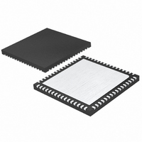
LTC2755BIUP-16#PBF Linear Technology, LTC2755BIUP-16#PBF Datasheet - Page 9

LTC2755BIUP-16#PBF
Manufacturer Part Number
LTC2755BIUP-16#PBF
Description
IC DAC 16BIT CUR OUT 64-QFN
Manufacturer
Linear Technology
Datasheet
1.LTC2755IUP-12PBF.pdf
(24 pages)
Specifications of LTC2755BIUP-16#PBF
Settling Time
2µs
Number Of Bits
16
Data Interface
Parallel
Number Of Converters
4
Voltage Supply Source
Single Supply
Operating Temperature
-40°C ~ 85°C
Mounting Type
Surface Mount
Package / Case
64-QFN
Lead Free Status / RoHS Status
Lead free / RoHS Compliant
Power Dissipation (max)
-
Available stocks
Company
Part Number
Manufacturer
Quantity
Price
TYPICAL PERFORMANCE CHARACTERISTICS
LTC2755-12, LTC2755-14, LTC2755-16
PIN FUNCTIONS
S2 (Pin 1): Span I/O Bit 2. Pins S0, S1 and S2 are used
to program and to read back the output ranges of the
DACs.
I
I
GND (Pin 3): Shield Ground, provides necessary shielding
for I
D3-D11 (Pins 4-12): LTC2755-12 Only. DAC Input/Output
Data Bits. These I/O pins set and read back the DAC code.
D11 is the MSB.
D5-D13 (Pins 4-12): LTC2755-14 Only. DAC Input/Output
Data Bits. These I/O pins set and read back the DAC code.
D13 is the MSB.
D7-D15 (Pins 4-12): LTC2755-16 Only. DAC Input/Output
Data Bits. These I/O pins set and read back the DAC code.
D15 is the MSB.
GND (Pin 13): Shield Ground, provides necessary shielding
for I
I
I
V
Requires a 0.1μF bypass capacitor to GND.
A2 (Pin 16): DAC Address Bit 2. See Table 3.
A1 (Pin 17): DAC Address Bit 1. See Table 3.
OUT2A
OUT2A
OUT2D
OUT2D
DD
OUT2A
OUT2D
(Pin 15): Positive Supply Input; 2.7V ≤ V
to ground.
(Pin 2): DAC A Current Output Complement. Tie
(Pin 14): DAC D Current Output Complement. Tie
to ground.
. Tie to ground.
. Tie to ground.
2mV/DIV
5V/DIV
V
UPD
OUT
Midscale Glitch
RISING MAJOR CARRY TRANSITION.
FALLING TRANSITION IS SIMILAR OR BETTER.
1nV • s TYP
UNIPOLAR 5V OUTPUT RANGE
LT1469 OUTPUT AMPLIFIER
C FEEDBACK = 27pF
V DD = 5V, V REF = 5V
500ns/DIV
2755 G20
DD
≤ 5.5V.
WAVEFORM
A0 (Pin 18): DAC Address Bit 0. See Table 3.
GND (Pin 19): Ground. Tie to ground.
CLR (Pin 20): Asynchronous Clear. When CLR is taken
to a logic low, the data registers are reset to the zero-volt
code (V
REFD (Pin 21): Reference Input for DAC D. The imped-
ance looking into this pin is 10k to ground. For normal
operation tie this pin to the negative reference voltage at
the output of reference inverting amplifier A2 (see Typical
Applications). Typically –5V; accepts up to ±15V.
R
pin provides the translation of the output voltage range for
bipolar spans. Accepts up to ±15V; for normal operation
tie to the positive reference voltage at R
impedance looking into this pin is 20k to ground.
R
operation tie to the output of the I/V converter amplifi er
for DAC D (see Typical Applications). The DAC output
current from I
to the R
10k to ground.
I
ground when the DAC is operating and should reside at 0V.
For normal operation tie to the negative input of the I/V
converter amplifi er for DAC D (see Typical Applications).
OUT1D
250μV/DIV
SETTLING
OFSD
FBD
5V/DIV
GATED
UPD
(Pin 23): DAC D Feedback Resistor. For normal
(Pin 22): Bipolar Offset Network for DAC D. This
(Pin 24): DAC D Current Output. This pin is a virtual
Settling 0V to 10V
OUT
USING LT1469 AMP
C
0V TO 10V STEP
FBD
FEEDBACK
T
= 0V) for the present output range.
pin. The impedance looking into this pin is
A
= 25°C, unless otherwise noted.
OUT1D
= 12pF
500ns/DIV
fl ows through the feedback resistor
2755 G10
LTC2755
IN2
(Pin 32). The
9
2755f


