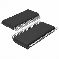
LTC2704IGW-14#PBF Linear Technology, LTC2704IGW-14#PBF Datasheet - Page 15

LTC2704IGW-14#PBF
Manufacturer Part Number
LTC2704IGW-14#PBF
Description
IC DAC 14BIT QUAD VOUT 44-SSOP
Manufacturer
Linear Technology
Datasheet
1.LTC2704IGW-12PBF.pdf
(22 pages)
Specifications of LTC2704IGW-14#PBF
Settling Time
9µs
Number Of Bits
14
Data Interface
Serial, SPI™
Number Of Converters
4
Voltage Supply Source
Analog and Digital, Dual ±
Operating Temperature
-40°C ~ 85°C
Mounting Type
Surface Mount
Package / Case
44-SSOP
Lead Free Status / RoHS Status
Lead free / RoHS Compliant
Power Dissipation (max)
-
Available stocks
Company
Part Number
Manufacturer
Quantity
Price
OPERATION
Examples
1. Using a 24-bit loading sequence, load DAC A with the
2. Using a 32-bit load sequence, load DAC C with bipolar
unipolar range of 0V to 10V, output at zero volts and all
other DACs with the bipolar range of ±10V, outputs at
zero volts. Note all DAC outputs should change at the
same time.
a) CS/LD↓
b) Clock SDI = 0010 1111 0000 0000 0000 0011
c) CS/LD↑
d) CS/LD↓
e) CS/LD↑
f) CS/LD↓
g) CS/LD↑
h) CS/LD↓
i) CS/LD↑
j) CS/LD↓
k) CS/LD↑
l) Alternatively steps j and k could be replaced with
± 2.5V and its output at zero volts. Use readback to
check B1 contents before updating the DAC output
(i.e., before copying B1 contents into B2).
a) CS/LD↓ (Note that after power-on, the Code in B1 is
b) Clock SDI = 0000 0000 0011 0100 1000 0000 0000
c) CS/LD↑
B1-Range of all DACs set to bipolar ±10V.
Clock SDI = 0010 0000 0000 0000 0000 0001
B1-Range of DAC A set to unipolar 0V to 10V.
Clock SDI = 0011 1111 1000 0000 0000 0000
B1-Code of all DACs set to midscale.
Clock SDI = 0011 0000 0000 0000 0000 0000
B1-Code of DAC A set to zero code.
Clock SDI = 0100 1111 XXXX XXXX XXXX XXXX
Update all DACs B1s into B2s for both Code and
Range.
LDAC
zero)
0000
B1-Code of DAC C set to midscale setting.
.
System Offset Adjustment
Many systems require compensation for overall system
offset, which may be an order of magnitude or more greater
than the excellent offset of the LTC2704.
The LTC2704 has individual offset adjust pins for each
of the four DACs. VOSA, VOSB, VOSC and VOSD are
referred to their corresponding signal grounds, AGNDA,
AGNDB, AGNDC and AGNDD. For noise immunity and
ease of adjustment, the control voltage is attenuated to
the DAC output:
The nominal input range of these pins is ±5V; other refer-
ence voltages of up to ±15V may be used if needed.
The VOSx pins have an input impedance of 1MΩ. To pre-
serve the settling performance of the LTC2704, these pins
d) CS/LD↓
e) Read Data out on SRO = 1000 0000 0000 0000
f) CS/LD↑
g) CS/LD↓
h) CS/LD↓
i) CS/LD↑
j) Alternatively steps h and i could be replaced with
V
V
–2.5V to 7.5V spans]
V
OS
OS
OS
Clock SDI = 0000 0000 0010 0100 0000 0000 0000
0100
Verifi es that B1-Code DAC C is at midscale setting.
B1-Range of DAC C set to Bipolar ±2.5V range.
Clock SDI = 0000 0000 1010 0100 xxxx xxxx xxxx
xxxx
Data Out on SRO = 0000 0000 0000 0100
Verifi es that B1-Range of DAC C set to Bipolar ±2.5V
Range.
CS/LD↑
Clock SDI = 0000 0000 0100 0100 xxxx xxxx xxxx
xxxx
Update DAC C B1 into B2 for both Code and Range
LDAC
= –0.01 • V(VOSx) [0V to 5V, ±2.5V spans]
= –0.02 • V(VOSx) [0V to 10V, ±5V,
= –0.04 • V(VOSx) [±10V span]
.
LTC2704
15
2704fc


