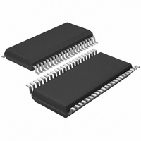
LTC2704IGW-14#PBF Linear Technology, LTC2704IGW-14#PBF Datasheet - Page 9

LTC2704IGW-14#PBF
Manufacturer Part Number
LTC2704IGW-14#PBF
Description
IC DAC 14BIT QUAD VOUT 44-SSOP
Manufacturer
Linear Technology
Datasheet
1.LTC2704IGW-12PBF.pdf
(22 pages)
Specifications of LTC2704IGW-14#PBF
Settling Time
9µs
Number Of Bits
14
Data Interface
Serial, SPI™
Number Of Converters
4
Voltage Supply Source
Analog and Digital, Dual ±
Operating Temperature
-40°C ~ 85°C
Mounting Type
Surface Mount
Package / Case
44-SSOP
Lead Free Status / RoHS Status
Lead free / RoHS Compliant
Power Dissipation (max)
-
Available stocks
Company
Part Number
Manufacturer
Quantity
Price
PIN FUNCTIONS
CS/LD (Pin 10): Synchronous Chip Select and Load Pin.
SDI (Pin 11): Serial Data Input. Data is clocked in on the
rising edge of the serial clock when CS/LD is low.
SRO (Pin 12): Serial Readback Data Output. Data is clocked
out on the falling edge of SCK. Readback data begins
clocking out after the last address bit A0 is clocked in.
SCK (Pin 13): Serial Clock.
CLR (Pin 14): Asynchronous Clear Pin. When this pin is
low, all code and span B2 registers are cleared to zero.
All DAC outputs are cleared to zero volts.
RFBD (Pin 16): DAC D Voltage Output Feedback Resis-
tor Pin.
OUTD (Pin 17): DAC D Voltage Output Pin. For best load
regulation, this open-loop amplifi er output is connected
to RFBD as close to the load as possible.
C1D (Pin 18): Feedback Capacitor Connection for DAC
D Output. This pin provides direct access to the negative
input of the channel D output amplifi er.
VOSD (Pin 19): Offset Adjust for DAC D. Nominal input
range is ±5V. V
±2.5V modes]. See Operation section.
AGNDD (Pin 20): DAC D Signal Ground. High impedance
input, does not carry supply currents. Tie to clean analog
ground.
REFG2 (Pin 21): Reference 2 Ground. High impedance
input, does not carry supply currents. Tie to clean analog
ground.
REFM2 (Pin 23): Reference 2 Inverting Amp Output. The
gain from REF2 to REFM2 is –1. Can swing to within 0.5V
of the analog supplies V
REF2 (Pin 24): DAC C and DAC D Reference Input.
V
Typically 15V. 4.5V to 16.5V Range. Can be different from
V
AGNDC (Pin 26): DAC C Signal Ground. High impedance
input, does not carry supply currents. Tie to clean analog
ground.
+
+
2
1
.
(Pin 25): Analog Positive Supply for DACs C and D.
OS
(DAC D) = –0.01• V(VOSD) [0V to 5V,
+
/V
–
.
VOSC (Pin 27): Offset Adjust for DAC C. Nominal input
range is ±5V. V
±2.5V modes]. See Operation section.
C1C (Pin 28): Feedback Capacitor Connection for DAC C
Output. This pin provides direct access to the negative
input of the channel C output amplifi er.
OUTC (Pin 29): DAC C Voltage Output Pin. For best load
regulation, this open-loop amplifi er output is connected
to RFBC as close to the load as possible.
RFBC (Pin 30): DAC C Output Feedback Resistor Pin.
AGND (Pin 32): Analog Ground Pin. Tie to clean analog
ground.
GND (Pin 33): Ground Pin. Tie to clean analog ground.
V
RFLAG (Pin 35): Reset Flag Pin. An active low output is
asserted when there is a power on reset or a clear event.
Returns high when an update command is executed.
RFBB (Pin 37): DAC B Output Feedback Resistor Pin.
OUTB (Pin 38): DAC B Voltage Output Pin. For best load
regulation, this open-loop amplifi er output is connected
to RFBB as close to the load as possible.
C1B (Pin 39): Feedback Capacitor Connection for DAC B
Output. This pin provides direct access to the negative
input of the channel B output amplifi er.
VOSB (Pin 40): Offset Adjust for DAC B. Nominal input
range is ±5V. V
±2.5V modes]. See Operation section.
AGNDB (Pin 41): DAC B Signal Ground. High impedance
input, does not carry supply currents. Tie to clean analog
ground.
V
B. Typically 15V. 4.5V to 16.5V Range. Can be different
from V
REF1 (Pin 43): DAC A and DAC B Reference Input.
REFM1 (Pin 44): Reference 1 Inverting Amp Output. The
gain from REF1 to REFM1 is –1. Can swing to within 0.5V
of the analog supplies V
DD
+
1
(Pin 42): Analog Positive Supply for DACs A DND
(Pin 34): Logic Supply. 2.7V to 5.5V Range.
+
2
.
OS
OS
(DAC B) = –0.01 • V(VOSB) [0V to 5V,
(DAC C) = –0.01• V(VOSC) [0V to 5V,
+
/V
–
.
LTC2704
2704fc
9


