LTC2704IGW-14#PBF Linear Technology, LTC2704IGW-14#PBF Datasheet - Page 16
LTC2704IGW-14#PBF
Manufacturer Part Number
LTC2704IGW-14#PBF
Description
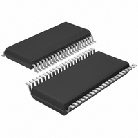
IC DAC 14BIT QUAD VOUT 44-SSOP
Manufacturer
Linear Technology
Datasheet
1.LTC2704IGW-12PBF.pdf
(22 pages)
Specifications of LTC2704IGW-14#PBF
Settling Time
9µs
Number Of Bits
14
Data Interface
Serial, SPI™
Number Of Converters
4
Voltage Supply Source
Analog and Digital, Dual ±
Operating Temperature
-40°C ~ 85°C
Mounting Type
Surface Mount
Package / Case
44-SSOP
Lead Free Status / RoHS Status
Lead free / RoHS Compliant
Power Dissipation (max)
-
Available stocks
Company
Part Number
Manufacturer
Quantity
Price


LTC2704
OPERATION
should be driven with a Thevenin-equivalent impedance
of 10kΩ or less. If not used, they should be shorted to
their respective signal grounds, AGNDx.
POWER-ON RESET AND CLEAR
When power is fi rst applied to the LTC2704, all DACs
power-up in 5V unipolar mode (S3 S2 S1 S0 = 0000). All
internal DAC registers are reset to 0 and the DAC outputs
are zero volts.
When the CLR pin is taken low, a system clear results. The
command and address shift registers, and the code and
confi guration B2 buffers, are reset to 0; the DAC outputs
are all reset to zero volts. The B1 buffers are left intact, so
that any subsequent “Update B1→B2” command (including
the use of LDAC) restores the addressed DACs to their
respective previous states.
If CLR is asserted during an operation, i.e., when CS/LD
is low, the operation is aborted. Integrity of the relevant
input (B1) buffers is not guaranteed under these condi-
tions, therefore the contents should be checked using
readback or replaced.
The RFLAG pin is used as a fl ag to notify the system of a
loss of data integrity. The RFLAG output is asserted low
at power-up, system clear, or if the logic supply V
16
DD
dips
below approximately 2V; and stays asserted until any valid
update command is executed.
SLEEP MODE
When a sleep command (C3 C2 C1 C0 = 1110) is issued,
the addressed DAC or DACs go into power-down mode.
DACs A and B share a reference inverting amplifi er as do
DACs C and D. If either DAC A or DAC B (similarly for DACs
C and D) is powered down, its shared reference inverting
amplifi er remains powered on. When both DAC A and DAC B
are powered down together, their shared reference invert-
ing amplifi er is also powered down (similarly for DACs C
and D). To determine the sleep status of a particular DAC,
a direct read span command is performed by addressing
the DAC and reading its status on the readback pin SRO.
The fi fth LSB is the sleep status bit (see Figures 2a and
2b). Table 4 shows the sleep status bit’s functionality.
Table 4. Readback Sleep Status Bit
SLP
0
1
STATUS
DAC n Awake
DAC n in Sleep Mode
2704fc
Related parts for LTC2704IGW-14#PBF
Image
Part Number
Description
Manufacturer
Datasheet
Request
R

Part Number:
Description:
IC,D/A CONVERTER,QUAD,12-BIT,CMOS,SOP,44PIN
Manufacturer:
Linear Technology
Datasheet:
Part Number:
Description:
IC,D/A CONVERTER,QUAD,16-BIT,CMOS,SOP,44PIN
Manufacturer:
Linear Technology
Datasheet:

Part Number:
Description:
IC DAC 12BIT QUAD VOUT 44-SSOP
Manufacturer:
Linear Technology
Datasheet:

Part Number:
Description:
IC DAC 16BIT QUAD VOUT 44-SSOP
Manufacturer:
Linear Technology
Datasheet:

Part Number:
Description:
IC DAC 12BIT QUAD VOUT 44-SSOP
Manufacturer:
Linear Technology
Datasheet:
Part Number:
Description:
IC DAC 14BIT QUAD VOUT 44-SSOP
Manufacturer:
Linear Technology
Datasheet:
Part Number:
Description:
IC DAC 16BIT QUAD VOUT 44-SSOP
Manufacturer:
Linear Technology
Datasheet:
Part Number:
Description:
IC,D/A CONVERTER,QUAD,12-BIT,CMOS,SOP,44PIN
Manufacturer:
Linear Technology
Part Number:
Description:
IC,D/A CONVERTER,QUAD,14-BIT,CMOS,SOP,44PIN
Manufacturer:
Linear Technology
Part Number:
Description:
IC,D/A CONVERTER,QUAD,14-BIT,CMOS,SOP,44PIN
Manufacturer:
Linear Technology
Part Number:
Description:
IC,D/A CONVERTER,QUAD,16-BIT,CMOS,SOP,44PIN
Manufacturer:
Linear Technology

Part Number:
Description:
Ltc2704-14 - Quad 14-bit Voltage Output Softspan Dac With Readback
Manufacturer:
Linear Technology Corporation
Datasheet:
Part Number:
Description:
Voltage Output SoftSpan DACs
Manufacturer:
Linear Technology
Datasheet:

Part Number:
Description:
16-/14-/12-Bit VOUT DACs in 3mm � 3mm DFN
Manufacturer:
LINER [Linear Technology]
Datasheet:
Part Number:
Description:
CD ROM LINEARVIEW DATASHEETS
Manufacturer:
Linear Technology