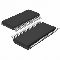
LTC2704IGW-14#PBF Linear Technology, LTC2704IGW-14#PBF Datasheet - Page 4

LTC2704IGW-14#PBF
Manufacturer Part Number
LTC2704IGW-14#PBF
Description
IC DAC 14BIT QUAD VOUT 44-SSOP
Manufacturer
Linear Technology
Datasheet
1.LTC2704IGW-12PBF.pdf
(22 pages)
Specifications of LTC2704IGW-14#PBF
Settling Time
9µs
Number Of Bits
14
Data Interface
Serial, SPI™
Number Of Converters
4
Voltage Supply Source
Analog and Digital, Dual ±
Operating Temperature
-40°C ~ 85°C
Mounting Type
Surface Mount
Package / Case
44-SSOP
Lead Free Status / RoHS Status
Lead free / RoHS Compliant
Power Dissipation (max)
-
Available stocks
Company
Part Number
Manufacturer
Quantity
Price
LTC2704
ELECTRICAL CHARACTERISTICS
temperature range, otherwise specifi cations are T
REFG1 = REFG2 = GND = 0V.
SYMBOL PARAMETER
SR
The
V
SYMBOL
Reference Inputs
Resistances
R
R
R
AC Performance (Note 4)
Power Supply
I
I
V
V
V
Digital Inputs/Outputs
V
V
V
V
I
4
DD
S
IN
VOSX
DD
+
–
IH
IL
OH
OL
+
REF1,
FBx
1
1
/V
= V
l
+
2
R
denotes specifi cations which apply over the full operating temperature range, otherwise specifi cations are T
+
REF2
2
= 15V, V
Slew Rate
Capacitive Load
Driving
–
PARAMETER
REF1, REF2 Input Voltage
Reference Input Resistance
Output Feedback Resistance
Offset Adjust Input Resistance
Glitch Impulse
Crosstalk
Digital Feedthrough
Multiplying Feedthrough Error
Multiplying Bandwidth
Output Noise Voltage Density
Output Noise Voltage
Supply Current, V
Supply Current, V
Logic Supply Voltage
Positive Analog Supply Voltage
Negative Analog Supply Voltage
Digital Input High Voltage
Digital Input Low Voltage
Digital Output High Voltage
Digital Output Low Voltage
Digital Input Current
= –15V, V
DD
= 5V, REF1 = REF2 = 5V, AGND = AGNDx = REFG1 = REFG2 = GND = 0V.
CONDITIONS
R
R
Within Maximum Load Current
L
L
DD
+
= 2k, V
= 2k, V
/V
–
+
+
/V
/V
–
–
= ±15V (Note 2)
= ±5V (Note 2)
A
CONDITIONS
V
0V to 5V Range, Midscale Transition
10V Step on V
±10V Range, Midscale
0V to 10V Range, V
Span = 0V to 5V, Full Scale
Span = 0V to 10V, Full Scale
10kHz
0.1Hz to 10Hz
Digital Inputs = 0V or V
V
V
Sleep Mode—All DACs (Note 4)
V
V
V
V
I
I
= 25°C, V
OH
OL
+
+
+
DD
DD
DD
DD
/V
/V
DAC B: 0V to 5V Range, Full Scale
DAC B: 0V to 10V Range, Full Scale
Span = 0V to 5V, Midscale
Span = 0V to 10V, Midscale
/V
Span = 0V to 5V, Midscale
Span = 0V to 10V, Midscale
= 200μA
= 200μA
–
–
–
= 2.7V to 5.5V
= 2.7V to 3.3V
= 2.7V to 5.5V
= 4.5V to 5.5V
= ±15V , ±10%; V
= ±5V, ±10%; V
= ±15V, 0V to 5V Span (Note 2)
The
+
1
l
= V
OUTA
denotes specifi cations which apply over the full operating
+
2
REF
REF
= 15V, V
REF
l
l
= ±5V, 10kHz Sine Wave
DD
= 2V, V
= 5V , V
MIN TYP
2.2
2.0
LTC2704-12
–
OUT
OUT
1000
= –15V, V
2.8
3
= 0V (Note 2)
= 0V (Note 2)
MAX
DD
= 5V, REF1 = REF2 = 5V, AGND = AGNDx =
MIN TYP
2.2
2.0
LTC2704-14
l
l
l
l
l
l
l
l
l
l
l
l
l
l
l
l
l
1000
2.8
3
V
CC
–14.5
–16.5
MIN
700
2.7
4.5
2.4
2.0
5
7
– 0.4
MAX MIN TYP MAX
0.001
1000
0.35
17.5
17.0
2.2
2.0
TYP
300
250
0.2
0.8
1.2
0.5
10
30
50
7
2
2
3
LTC2704-16
A
1000
2.8
= 25°C,
3
MAX
14.5
16.5
–4.5
5.5
0.6
0.8
0.4
20
18
±1
2
1
μV/√Hz
μV/√Hz
UNITS
μV
μV
mV
UNITS
2704fc
nV-s
nV-s
nV-s
nV-s
V/μs
V/μs
RMS
RMS
kHz
kHz
mA
mA
mA
kΩ
kΩ
kΩ
P-P
μA
μA
pF
V
V
V
V
V
V
V
V
V
V


