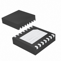
DS4424N+T&R Maxim Integrated Products, DS4424N+T&R Datasheet - Page 6

DS4424N+T&R
Manufacturer Part Number
DS4424N+T&R
Description
IC DAC 7BIT 4CH 5.5V 14-TDFN
Manufacturer
Maxim Integrated Products
Datasheet
1.DS4422NTR.pdf
(11 pages)
Specifications of DS4424N+T&R
Number Of Bits
7
Data Interface
Serial
Number Of Converters
4
Voltage Supply Source
Single Supply
Operating Temperature
-40°C ~ 85°C
Mounting Type
Surface Mount
Package / Case
14-TDFN Exposed Pad
Lead Free Status / RoHS Status
Lead free / RoHS Compliant
Power Dissipation (max)
-
Settling Time
-
The DS4422/DS4424 contain two or four I
current sources that are each capable of sinking and
sourcing current. Each output (OUT0, OUT1, OUT2, and
OUT3) has 127 sink and 127 source settings that can be
controlled by the I
and corresponding step sizes of the outputs are deter-
mined by external resistors, connected to pins FS0, FS1,
FS2, and FS3, that can adjust the output current over a
4:1 range. Pins OUT2, OUT3, FS2, and FS3 are only
available on the DS4424.
The formula to determine R
pins) to attain the desired full-scale current range is:
Equation 1:
Where I
the R
table), and R
To calculate the output current value (I
corresponding DAC value (see Table 1 for corresponding
memory addresses), use equation 2.
Equation 2:
On power-up the DS4422/DS4424 output zero current.
This is done to prevent them from sinking or sourcing an
incorrect amount of current before the system host con-
troller has had a chance to modify the device’s setting.
As a source for biasing instrumentation or other circuits,
the DS4422/DS4424 provide a simple and inexpensive
current source with an I
adjustable full-scale range allows the application to get
the most out of its 7-bit sink or source resolution.
When used in adjustable power-supply applications
(see Typical Operating Circuit ), the DS4422/DS4424 do
not affect the initial power-up voltage of the supply
because they default to providing zero output current on
power-up. As the devices source or sink current into the
feedback-voltage node, they change the amount of out-
put voltage required by the regulator to reach its steady-
state operating point. Using the external resistor, R
set the output current range, the DS4422/DS4424 pro-
vide some flexibility for adjusting the impedances of the
feedback network or the range over which the power
supply can be controlled or margined.
Two-/Four-Channel, I
Current DAC
6
_______________________________________________________________________________________
FS
FS
voltage (see the DC Electrical Characteristics
is the desired full-scale current value, V
FS
I
OUT
is the external resistor value.
R
=
2
FS
C interface. The full-scale ranges
D
AC Value dec
Detailed Description
=
16 I
2
V
1
C interface for control. The
RFS
×
27
FS
FS
(
(connected to the FSx
× 127
)
OUT
×
I
FS
) based on the
2
C adjustable
2
RFS
FS
C, 7-Bit Sink/Source
, to
is
The DS4422/DS4424 respond to one of four I
addresses determined by the two address inputs, A0
and A1. The address inputs should be connected to
either V
determined by the address input combinations.
Table 1. Slave Addresses
To control the DS4422/DS4424’s current sources, write
to the memory addresses listed in Table 2.
Table 2. Memory Addresses
The format of each output control register is given by:
Where:
*Only for DS4424.
BIT
D
MSB
S
X
S
GND
GND
V
V
A1
MEMORY ADDRESS
CC
CC
NAME
Data
Sign
CC
Bit
D
6
or ground. Table 1 lists the slave addresses
(HEX)
FAh*
FBh*
F8h
F9h
Determines if DAC sources or
sinks current. For sink
S = 0; for source S = 1.
7-Bit Data Controlling DAC
Output. Setting 0000000b
outputs zero current regardless
of the state of the sign bit.
GND
GND
V
V
A0
CC
CC
D
5
FUNCTION
D
4
Memory Organization
D
SLAVE ADDRESS
3
I
CURRENT SOURCE
2
C Slave Address
(HEX)
D
A0h
20h
60h
E0h
2
OUT2*
OUT3*
OUT0
OUT1
POWER-ON
D
DEFAULT
0000000b
1
2
C slave
0b
LSB
D
0


