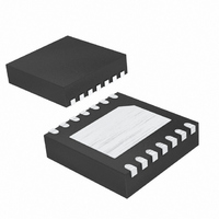
DS4424N+T&R Maxim Integrated Products, DS4424N+T&R Datasheet - Page 7

DS4424N+T&R
Manufacturer Part Number
DS4424N+T&R
Description
IC DAC 7BIT 4CH 5.5V 14-TDFN
Manufacturer
Maxim Integrated Products
Datasheet
1.DS4422NTR.pdf
(11 pages)
Specifications of DS4424N+T&R
Number Of Bits
7
Data Interface
Serial
Number Of Converters
4
Voltage Supply Source
Single Supply
Operating Temperature
-40°C ~ 85°C
Mounting Type
Surface Mount
Package / Case
14-TDFN Exposed Pad
Lead Free Status / RoHS Status
Lead free / RoHS Compliant
Power Dissipation (max)
-
Settling Time
-
Example: R
a value of 0xAAh. Calculate the output current.
The MSB of the output register is 1, so the output is
sourcing the value corresponding to position 2Ah (42
decimal). The magnitude of the output current is equal to:
The following terminology is commonly used to describe
I
I
DS4422/DS4424 is determined by the state of the A0
and A1 pins (see Table 1).
Master Device: The master device controls the slave
devices on the bus. The master device generates SCL
clock pulses and START and STOP conditions.
Slave Devices: Slave devices send and receive data
at the master’s request.
Bus Idle or Not Busy: Time between STOP and START
conditions when both SDA and SCL are inactive and in
their logic-high states. When the bus is idle it often initi-
ates a low-power mode for slave devices.
START Condition: A START condition is generated by
the master to initiate a new data transfer with a slave.
Transitioning SDA from high to low while SCL remains
high generates a START condition. See Figure 1 for
applicable timing.
Figure 1. I
2
2
C data transfers:
C Slave Address: The slave address of the
SDA
SCL
NOTE: TIMING IS REFERENCED TO V
I
2
I
FS
C Serial Interface Description
STOP
2
= (0.976V/80kΩ) x (127/16) = 96.838µA
C Timing Diagram
FS0
96.838µA x (42/127) = 32.025µA
t
BUF
= 80kΩ and register 0xF8h is written to
START
Two-/Four-Channel, I
_______________________________________________________________________________________
IL(MAX)
t
t
HD:STA
LOW
AND V
IH(MIN)
.
I
t
2
R
t
HD:DAT
C Definitions
t
F
t
HIGH
t
SU:DAT
STOP Condition: A STOP condition is generated by the
master to end a data transfer with a slave. Transitioning
SDA from low to high while SCL remains high generates
a STOP condition. See Figure 1 for applicable timing.
Repeated START Condition: The master can use a
repeated START condition at the end of one data trans-
fer to indicate that it will immediately initiate a new data
transfer following the current one. Repeated STARTs are
commonly used during read operations to identify a spe-
cific memory address to begin a data transfer. A repeat-
ed START condition is issued identically to a normal
START condition. See Figure 1 for applicable timing.
Bit Write: Transitions of SDA must occur during the low
state of SCL. The data on SDA must remain valid and
unchanged during the entire high pulse of SCL, plus the
setup and hold time requirements (Figure 1). Data is
shifted into the device during the rising edge of the SCL.
Bit Read: At the end of a write operation, the master must
release the SDA bus line for the proper amount of setup
time (Figure 1) before the next rising edge of SCL during a
bit read. The device shifts out each bit of data on SDA at
the falling edge of the previous SCL pulse and the data bit
is valid at the rising edge of the current SCL pulse.
Remember that the master generates all SCL clock puls-
es, including when it is reading bits from the slave.
Acknowledgement (ACK and NACK): An Acknowledge-
ment (ACK) or Not Acknowledge (NACK) is always the
ninth bit transmitted during a byte transfer. The device
receiving data (the master during a read or the slave
during a write operation) performs an ACK by transmit-
ting a zero during the ninth bit. A device performs a
REPEATED
2
START
C, 7-Bit Sink/Source
t
SU:STA
t
HD:STA
Current DAC
t
SP
t
SU:STO
7


