LM5067MMX-1 National Semiconductor, LM5067MMX-1 Datasheet - Page 14
LM5067MMX-1
Manufacturer Part Number
LM5067MMX-1
Description
Manufacturer
National Semiconductor
Datasheet
1.LM5067MMX-1.pdf
(24 pages)
Specifications of LM5067MMX-1
Linear Misc Type
Negative Voltage
Family Name
LM5067-1
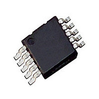
Package Type
MSOP
Operating Supply Voltage (min)
-9V
Operating Supply Voltage (max)
-80V
Operating Temperature (min)
-40C
Operating Temperature (max)
125C
Operating Temperature Classification
Automotive
Product Depth (mm)
3mm
Product Height (mm)
0.86mm
Product Length (mm)
3mm
Mounting
Surface Mount
Pin Count
10
Lead Free Status / Rohs Status
Not Compliant
Available stocks
Company
Part Number
Manufacturer
Quantity
Price
Company:

Part Number:
LM5067MMX-1/NOPB
Manufacturer:
st
Quantity:
47


www.national.com
Under-Voltage Lock-Out (UVLO)
The series pass MOSFET (Q1) is enabled when the input
supply voltage (V
the programmable under-voltage lockout (UVLO) and over-
voltage lock-out (OVLO) levels. Typically the UVLO level at
V
1. When V
current sink at UVLO/EN is enabled, the current source at
OVLO is off, and Q1 is held off by the 2.2 mA pull-down cur-
rent at the GATE pin. V
voltage at the UVLO/EN pin reaches 2.5V above VEE. Upon
reaching the UVLO level, the 22 µA current sink at the UVLO/
EN pin is switched off, increasing the voltage at the pin, pro-
viding hysteresis for this threshold. With the UVLO/EN pin
above 2.5V, Q1 is switched on by the 52 µA current source at
the GATE pin.
See the Applications Section for a procedure to calculate the
values of the threshold setting resistors (R1-R3). The mini-
mum possible UVLO level can be set by connecting the
UVLO/EN pin to VCC. In this case Q1 is enabled when the
operating voltage (VCC – VEE) reaches the POR
(8.4V).
Over-Voltage Lock-Out (OVLO)
The series pass MOSFET (Q1) is enabled when the input
supply voltage (V
the programmable under-voltage lockout (UVLO) and over-
voltage lock-out (OVLO) levels. Typically the OVLO level at
V
1. If V
VEE Q1 is switched off by the 2.2 mA pull-down current at the
GATE pin, denying power to the load. When the OVLO pin is
above 2.5V, the internal 22 µA current source at OVLO is
switched on, raising the voltage at OVLO and providing
threshold hysteresis. When the voltage at the OVLO pin is
reduced below 2.5V the 22 µA current source is switched off,
and Q1 is enabled. See the Applications Section for a proce-
dure to calculate the threshold setting resistor values.
SYS
SYS
is set with a resistor divider (R1-R3) as shown in Figure
is set with a resistor divider (R1-R3) as shown in Figure
SYS
raises the OVLO pin voltage more than 2.5V above
SYS
is less than the UVLO level, the internal 22 µA
SYS
SYS
) is within the operating range defined by
) is within the operating range defined by
SYS
reaches its UVLO level when the
FIGURE 6. Restart Sequence (LM5067-2)
EN
threshold
14
Shutdown/Enable Control
See the Applications Information section for a description of
how to use the UVLO/EN pin and/or the OVLO pin for remote
shutdown and enable control of the LM5067.
Power Good Pin
The Power Good output indicator pin (PGD) is connected to
the drain of an internal N-channel MOSFET. An external pull-
up resistor is required at PGD to an appropriate voltage to
indicate the status to downstream circuitry. The off-state volt-
age at the PGD pin must be more positive than VEE, and can
be up to 80V above VEE with transient capability to 100V.
PGD is switched high at the end of the turn-on sequence when
the voltage from OUT to SENSE (the external MOSFET’s
V
MOSFET’s V
age goes below the UVLO threshold or above the OVLO
threshold, or if a fault is detected. The PGD output is high
when the operating voltage (VCC-VEE) is less than 2V.
Application Information
(Refer to Figure 1)
R
The LM5067 operating voltage is determined by an internal
13V shunt regulator which receives its current from the sys-
tem voltage via R
the LM5067 operating voltage (VCC – VEE) is between VEE
and VEE+13V. The remainder of the system voltage is
dropped across the input resistor R
to pass at least 2 mA into the LM5067 at the minimum system
voltage. The resistor’s power rating must be selected based
on the power dissipation at maximum system voltage, calcu-
lated from:
CURRENT LIMIT, R
The LM5067 monitors the current in the external MOSFET
(Q1) by measuring the voltage across the sense resistor
DS
IN
, C
) decreases below 1.23V. PGD switches low if the
IN
DS
P
increases past 2.5V, if the system input volt-
RIN
IN
. When the system voltage exceeds 13V,
S
= (V
SYS(max)
– 13V)
IN
, which must be selected
30030933
2
/R
IN
Related parts for LM5067MMX-1
Image
Part Number
Description
Manufacturer
Datasheet
Request
R

Part Number:
Description:
National Semiconductor [8-Bit D/A Converter]
Manufacturer:
National Semiconductor
Datasheet:
Part Number:
Description:
National Semiconductor [Media Coprocessor]
Manufacturer:
National Semiconductor
Datasheet:
Part Number:
Description:
Digitally Controlled Tone and Volume Circuit with Stereo Audio Power Amplifier, Microphone Preamp Stage and National 3D Sound
Manufacturer:
National Semiconductor
Datasheet:
Part Number:
Description:
Digitally Controlled Tone and Volume Circuit with Stereo Audio Power Amplifier, Microphone Preamp Stage and National 3D Sound
Manufacturer:
National Semiconductor
Datasheet:
Part Number:
Description:
AC97 Rev 2 Codec with Sample Rate Conversion and National 3D Sound
Manufacturer:
National Semiconductor
Part Number:
Description:
Manufacturer:
National Semiconductor
Datasheet:
Part Number:
Description:
Manufacturer:
National Semiconductor
Datasheet:
Part Number:
Description:
General Purpose, Low Voltage, Low Power, Rail-to-Rail Output Operational Amplifiers
Manufacturer:
National Semiconductor
Datasheet:
Part Number:
Description:
8-bit 20 MSPS flash A/D converter.
Manufacturer:
National Semiconductor
Datasheet:
Part Number:
Description:
Low Noise Quad Operational Amplifier
Manufacturer:
National Semiconductor
Datasheet:
Part Number:
Description:
Quad Differential Line Receivers
Manufacturer:
National Semiconductor
Datasheet:
Part Number:
Description:
Quad High Speed Trapezoidal? Bus Transceiver
Manufacturer:
National Semiconductor
Datasheet:
Part Number:
Description:
Dual Line Receiver
Manufacturer:
National Semiconductor
Datasheet:
Part Number:
Description:
TTL to 10k ECL Level Translator with Latch
Manufacturer:
National Semiconductor
Datasheet: