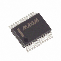
MAX503CAG+T Maxim Integrated Products, MAX503CAG+T Datasheet - Page 14

MAX503CAG+T
Manufacturer Part Number
MAX503CAG+T
Description
IC DAC 10BIT 5V LP 24-SSOP
Manufacturer
Maxim Integrated Products
Datasheet
1.MAX503CNG.pdf
(16 pages)
Specifications of MAX503CAG+T
Settling Time
25µs
Number Of Bits
10
Data Interface
Parallel
Number Of Converters
1
Voltage Supply Source
Dual ±
Power Dissipation (max)
640mW
Operating Temperature
0°C ~ 70°C
Mounting Type
Surface Mount
Package / Case
24-SSOP
Lead Free Status / RoHS Status
Lead free / RoHS Compliant
5V, Low-Power, Parallel-Input,
Voltage-Output, 10-Bit DAC
Table 3. Unipolar Binary Code Table
(0V to V
* Write 10-bit data words with two sub-LSB 0s because the
A -V
necting ROFS to REFIN and RFB to VOUT, and operat-
ing from dual (±5V) supplies (Figure 11). Table 5
shows the DAC-latch contents (input) vs. VOUT (out-
put). In this range, 1LSB = V
The MAX503 can be used as a four-quadrant multiplier
by connecting ROFS to REFIN and RFB to VOUT, and
using (1) an offset binary digital code, (2) bipolar
power supplies, and (3) a bipolar analog input at
REFIN within the range V
in Figure 12.
In general, a 10-bit DAC’s output is D(V
where “G” is the gain (1 or 2) and “D” is the binary rep-
resentation of the digital input divided by 2
This formula is precise for unipolar operation. However,
for bipolar, offset binary operation, the MSB is really a
polarity bit. No resolution is lost because the number of
steps is the same. The output voltage, however, has
been shifted from a range of, for example, 0V to
4.096V (G = 2) to a range of -2.048V to +2.048V.
Keep in mind that when using the DAC as a four-quad-
rant multiplier, the scale is skewed. The negative full
scale is -V
+V
14
DAC input latch is 12 bits wide.
REFIN
REFIN
______________________________________________________________________________________
1111
1000
1000
0111
0000
0000
- 1LSB.
INPUT*
REFIN
to +V
1111
0000
0000
1111
0000
0000
REFIN
REFIN
11(00)
01(00)
11(00)
01(00)
00(00)
00(00)
Four-Quadrant Multiplication
Output), Gain = 1
, while the positive full scale is
bipolar range is set up by con-
SS
Bipolar Configuration
+ 2V to V
REFIN
(V
REFIN
(V
(V
(V
(V
REFIN
REFIN
OUTPUT
REFIN
REFIN
(2
)
1024
512
OV
-9
DD
)
)
)
)
1024
1024
1024
1023
1024
511
).
513
= +V
1
- 2V, as shown
REFIN
10
REFIN
or 1,024.
/2
)(G),
Table 4. Unipolar Binary Code Table
(0V to 2V
* Write 10-bit data words with two sub-LSB 0s because the
Table 5. Bipolar (Offset Binary) Code
Table (-V
* Write 10-bit data words with two sub-LSB 0s because the
DAC input latch is 12 bits wide.
DAC input latch is 12 bits wide.
1111
1000
1000
0111
0000
1111
1000
1000
0111
0000
0000
0000
INPUT*
INPUT*
1111
0000
0000
1111
0000
1111
0000
0000
1111
0000
0000
0000
REFIN
REFIN
11(00)
01(00)
00(00)
11(00)
01(00)
11(00)
01(00)
00(00)
11(00)
00(00)
00(00)
01(00)
to +V
Output), Gain = 2
REFIN
+2 (V
+2 (V
+2 (V
+2 (V
+2 (V
(+V
(+V
(-V
(-V
(-V
REFIN
REFIN
REFIN
REFIN
REFIN
OUTPUT
REFIN
OUTPUT
REFIN
REFIN
REFIN
REFIN
Output)
OV
)
0V
)
)
)
)
)
)
)
)
)
1024
511
1024
1023
1024
1024
1024
512
512
511
512
512
512
511
512
513
512
1
1
1
= -V
= +V
REFIN
REFIN


