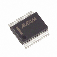
MAX503CAG+T Maxim Integrated Products, MAX503CAG+T Datasheet - Page 8

MAX503CAG+T
Manufacturer Part Number
MAX503CAG+T
Description
IC DAC 10BIT 5V LP 24-SSOP
Manufacturer
Maxim Integrated Products
Datasheet
1.MAX503CNG.pdf
(16 pages)
Specifications of MAX503CAG+T
Settling Time
25µs
Number Of Bits
10
Data Interface
Parallel
Number Of Converters
1
Voltage Supply Source
Dual ±
Power Dissipation (max)
640mW
Operating Temperature
0°C ~ 70°C
Mounting Type
Surface Mount
Package / Case
24-SSOP
Lead Free Status / RoHS Status
Lead free / RoHS Compliant
The MAX503 consists of a parallel-input logic interface, a
10-bit R-2R ladder, a reference, and an op amp. The
Functional Diagram shows the control lines and signal
flow through the input data latch to the DAC latch, as well
as the 2.048V reference and output op amp. Total supply
current is typically 250µA with a single +5V supply. This
circuit is ideal for battery-powered, microprocessor-con-
trolled applications where high accuracy, no adjustments,
and minimum component count are key requirements.
The MAX503 uses an “inverted” R-2R ladder network with
a BiCMOS op amp to convert 10-bit digital data to analog
voltage levels. Figure 1 shows a simplified diagram of the
R-2R DAC and op amp. Unlike a standard DAC, the
MAX503 uses an “inverted” ladder network. Normally, the
REFIN pin is the current output of a standard DAC and
would be connected to the summing junction, or virtual
ground, of an op amp. In this standard DAC configura-
tion, however, the output voltage would be the inverse of
5V, Low-Power, Parallel-Input,
Voltage-Output, 10-Bit DAC
Figure 1. Simplified MAX503 DAC Circuit
8
________________Detailed Description
REFGND
REFOUT
REFIN
AGND
2.048V
_______________________________________________________________________________________
D6/S0
2R
D7/S1
*
LATCH
INPUT
LSB
NBL
LSB
D8/D0
2R
R
D9/D1
2R
DAC LATCH
D2
LATCH
INPUT
D3
NBM
D4
R
D5
MAX503
2R
LATCH
*
INPUT
MSB
NBH
R
SHOWN FOR ALL 1s
R-2R Ladder
MSB
2R
2R
2R
R 80k
OUTPUT
BUFFER
CLR
ROFS
RFB
VOUT
the reference voltage. The MAX503’s topology makes the
ladder output voltage the same polarity as the reference
input, making the device suitable for single-supply oper-
ation. The BiCMOS op amp is then used to buffer, invert,
or amplify the ladder signal.
Ladder resistors are nominally 80kΩ to conserve power
and are laser trimmed for gain and linearity. The input
impedance at REFIN is code dependent. When the DAC
register is all 0s, all rungs of the ladder are grounded
and REFIN is open or no load. Maximum loading (mini-
mum REFIN impedance) occurs at code 010101....
Minimum reference input impedance at this code is guar-
anteed to be not less than 40kΩ.
The REFIN and REFOUT pins allow the user to choose
between driving the R-2R ladder with the on-chip refer-
ence or an external reference. REFIN may be below ana-
log ground when using dual supplies. See the External
Reference and Four-Quadrant Multiplication sections for
more information.
The on-chip reference is laser trimmed to generate
2.048V at REFOUT. The output stage can source and
sink current so REFOUT can settle to the correct volt-
age quickly in response to code-dependent loading
changes. Typically, source current is 5mA and sink
current is 100µA.
REFOUT connects the internal reference to the R-2R
DAC ladder at REFIN. The R-2R ladder draws 50µA
maximum load current. If any other connection is made
to REFOUT, ensure that the total load current is less
than 100µA to avoid gain errors.
A separate REFGND pin is provided to isolate refer-
ence currents from other analog and digital ground
currents. To achieve specified noise performance, con-
nect a 33µF capacitor from REFOUT to REFGND (see
Figure 2). Using smaller capacitance values increases
noise, and values less than 3.3µF may compromise the
reference’s stability. For applications requiring the low-
est noise, insert a buffered RC filter between REFOUT
and REFIN. When using the internal reference,
REFGND must be connected to AGND. In applications
not requiring the internal reference, connect REFGND
to V
typically 100µA of V
the need for C
DD
, which shuts down the reference. This saves
REFOUT
DD
.
supply current and eliminates
Internal Reference


