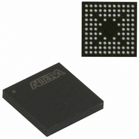
EPM240GM100C5N Altera, EPM240GM100C5N Datasheet

EPM240GM100C5N
Specifications of EPM240GM100C5N
Available stocks
Related parts for EPM240GM100C5N
EPM240GM100C5N Summary of contents
Page 1
... May not operate for V brown- CCINT out conditions at or below 2.1 V. Does not support Serial Vector File (.svf) format programming. Altera Corporation ES-M2EPM1270-1.3 MAX II Device Family Table 1. Affected Devices EPM240 revision F and earlier EPM240G revision G and earlier ...
Page 2
... See the “MAX II Power-up Issue”section for information on distinguishing revision codes. (2) Altera is offering permanent recommendations and workarounds for this issue. (3) This issue is a permanent programming file compatibility restriction. MAX II Power-up The MAX II devices may not power-up and enter user mode correctly for ...
Page 3
... V. This value is near the minimum operating voltage (1. the 1.8-V EPM2210G and EPM1270G devices and can lead to unintended device reset during user-mode operation or a failed in- system programming attempt. I Altera Corporation EPM2210G & EPM1270G Brown-out Voltage Issue Rise Times and V Noise/Dip Free Window (Continued) ...
Page 4
... UFM block does not support program/write or erase operations from the logic array interface Thresholds for Brown-Out Trigger Units 500 mA 300 mA is less than CCINT is less the threshold, you CCINT is less than CCINT Altera Corporation CCINT ...
Page 5
... The OSC output can be ANDed with the OSCENA port in the design to ensure that this port starts clocking when expected after power-up. Altera Corporation UFM block optional oscillator output port can exhibit a single high or low pulse after power-up Optional Schmitt trigger inputs may glitch for falling input signal edge rates greater than 1 µ ...
Page 6
... Right-click and select Locate in Assignment Editor. Double-click the cell under Assignment Name and select Input Delay from Pin to Internal Cells in the drop-down list. Double-click the Value cell to the right of the assignment name just made and enter 1. Click Save (File menu). Altera Corporation ...
Page 7
... V CCIO by pin 4 of the 10-pin header. This affects the voltage level of TCK driving the MAX II device. See the respective Altera download cable data sheet for more information. This issue can be avoided by ensuring that the download cable or third- party programming/JTAG hardware supplies a TCK fall time less than 50 ns when driving the combined load capacitance of the cable, JTAG header, and trace for TCK ...
Page 8
... V CCINT to dip or ring at or below 2.1 V. POR re-trigger voltage for CCINT ) compared to EPM1270 CONFIG . Actual device CC CONFIG for EPM1270 CONFIG POR Trip Voltage During (1) Brown-Out (1) 2.1 V 1.4 V Altera Corporation voltage time Table 5 ...
Page 9
... This brown-out POR trigger voltage rises to 1.55 V during DEV_OE de-assertion or in-system programming. Serial Vector File Support EPM1270 ES devices do not support SVF format for programming. The devices do support POF, Jam, and JBC file formats for programming with the Quartus II software. Altera Corporation EPM1270 ES ES Device Approximate Voltage for SRAM Download Start t CONFIG = 200 µ ...
Page 10
... Copyright © 2005 Altera Corporation. All rights reserved. Altera, The Programmable Solutions Company, the stylized Altera logo, specific device designations, and all other words and logos that are identified as trademarks and/or service marks are, unless noted otherwise, the trademarks and service marks of Altera Corporation in the U ...


